Supplier awards and collaboration projects
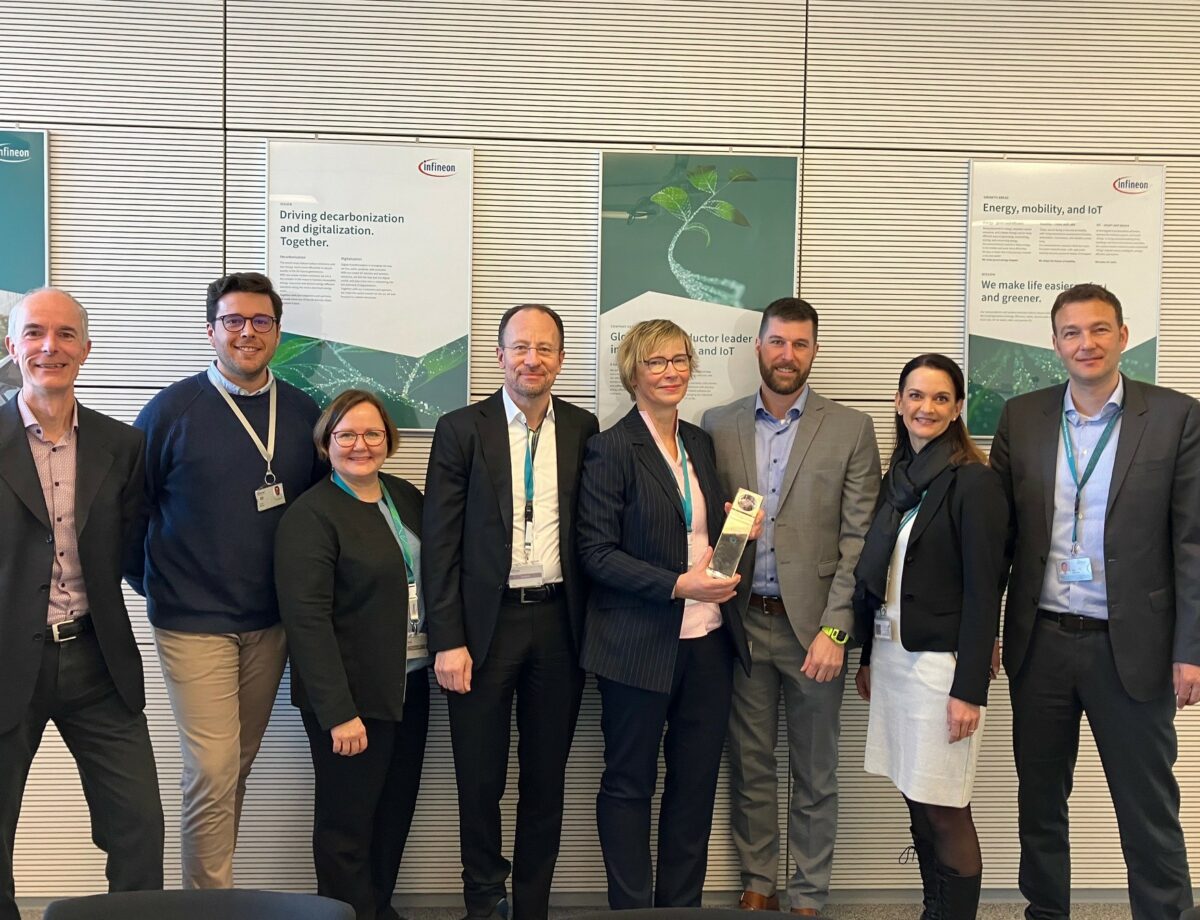
Infineon’s best wafer supplier award
We are honored to share that Okmetic has received semiconductor giant Infineon Technologies’ Best Wafer Supplier award 2023! In their statement, Infineon Technologies described Okmetic as extremely supportive, agile and flexible and continued that we really listened to their needs.
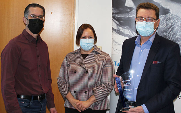
Appreciation award from Skyworks Singapore
Wireless semiconductor giant Skyworks Solutions awarded Okmetic with an Appreciation Award in recognition of our strategic partnership in 2021.
SilTerra Malaysia’s new manufacturing technology for MEMS and Photonics devices uses C-SOI® wafers as a platform
Okmetic is proud to support SilTerra Malaysia’s new manufacturing technology for microelectromechanical systems (“MEMS”) and Photonics devices with its Cavity Silicon-On-Insulator (“C-SOI®”) wafers.
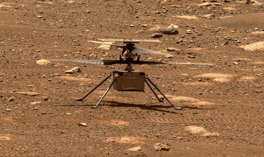
Mars exploration is enabled with sensor technology by Murata Finland using Okmetic’s advanced silicon wafer as a platform.
NASA’s Mars exploration is enabled with state-of-the-art sensor technology by Murata Finland using Okmetic’s advanced silicon wafer as a platform. Murata Finland’s SCA100T dual-axis inclinometer is used in NASA’s Ingenuity helicopter, which arrived to Mars with the Perseverance rover in February 2021.
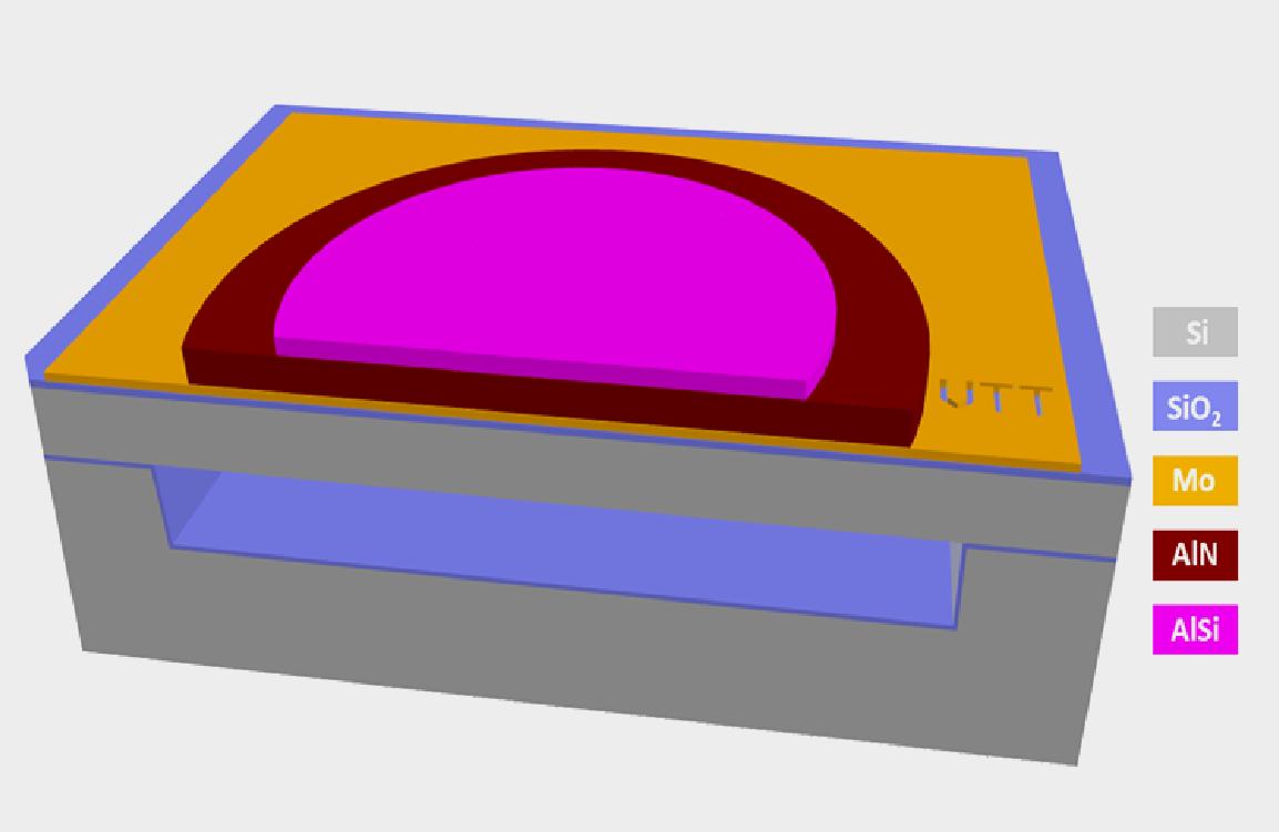
Enhancing PMUT performance with C-SOI® and EC-SOI wafers: Results from VTT – Okmetic collaboration
Okmetic-VTT collaboration examined PMUT performance and how C-SOI® and EC-SOI wafers impacted it. The findings are noteworthy, as the benefits extend to various MEMS devices, including CMUTs, timing devices and silicon photonics, where enhanced uniformity significantly improves sensitivity and measurement accuracy.
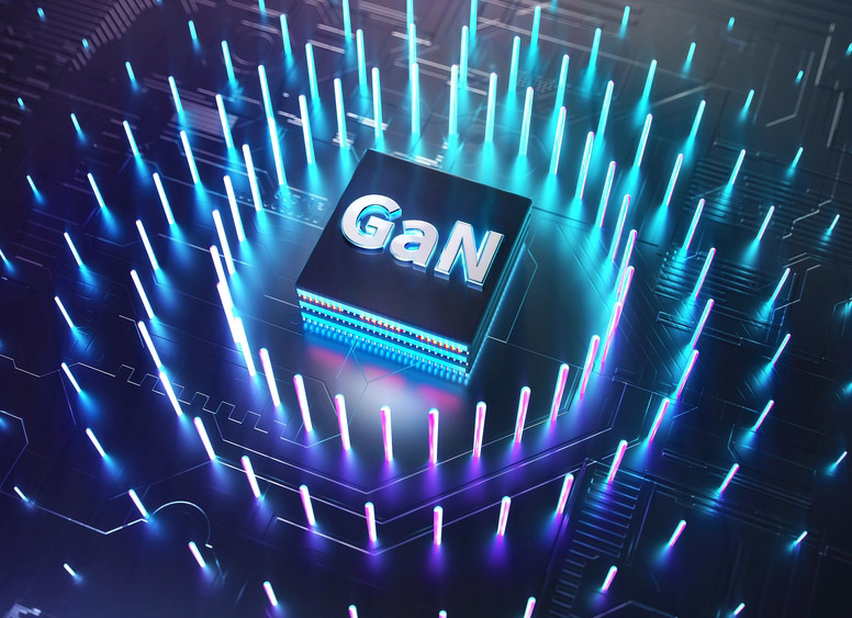
GaN-on-SOI collaboration with IMEC
IMEC successfully grew a 4.4 µm GaN-epi-stack on Okmetic wafers, with the GaN-optimized SOI wafers showing superior GaN layer uniformity, reduced wafer bowing, and enhanced electrical performance in post-growth studies.