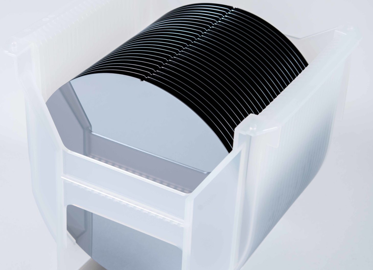
SSP wafers – Single Side Polished
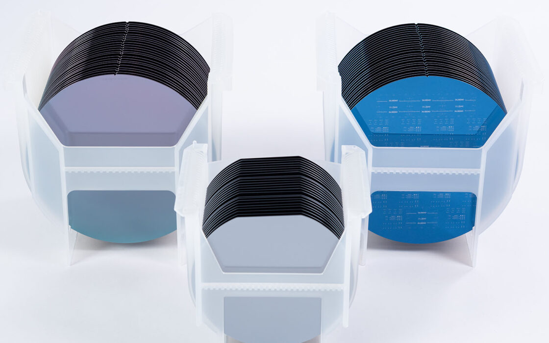
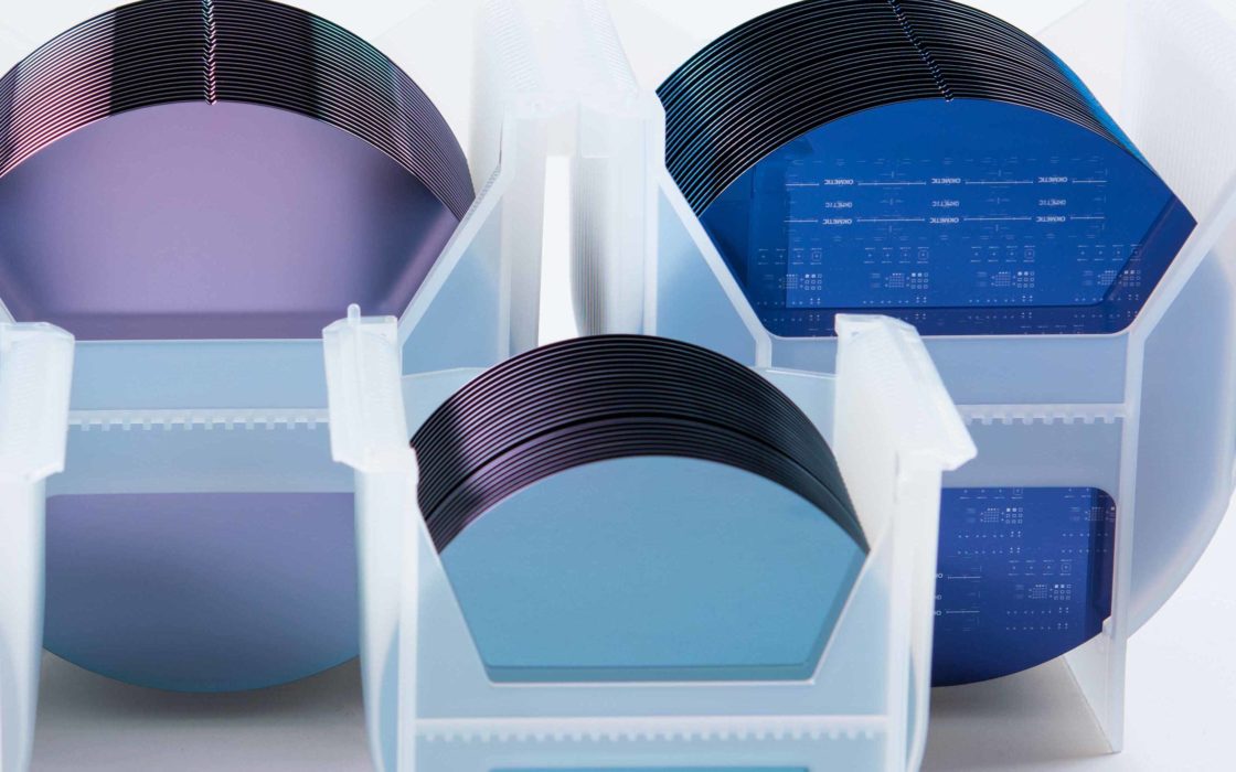
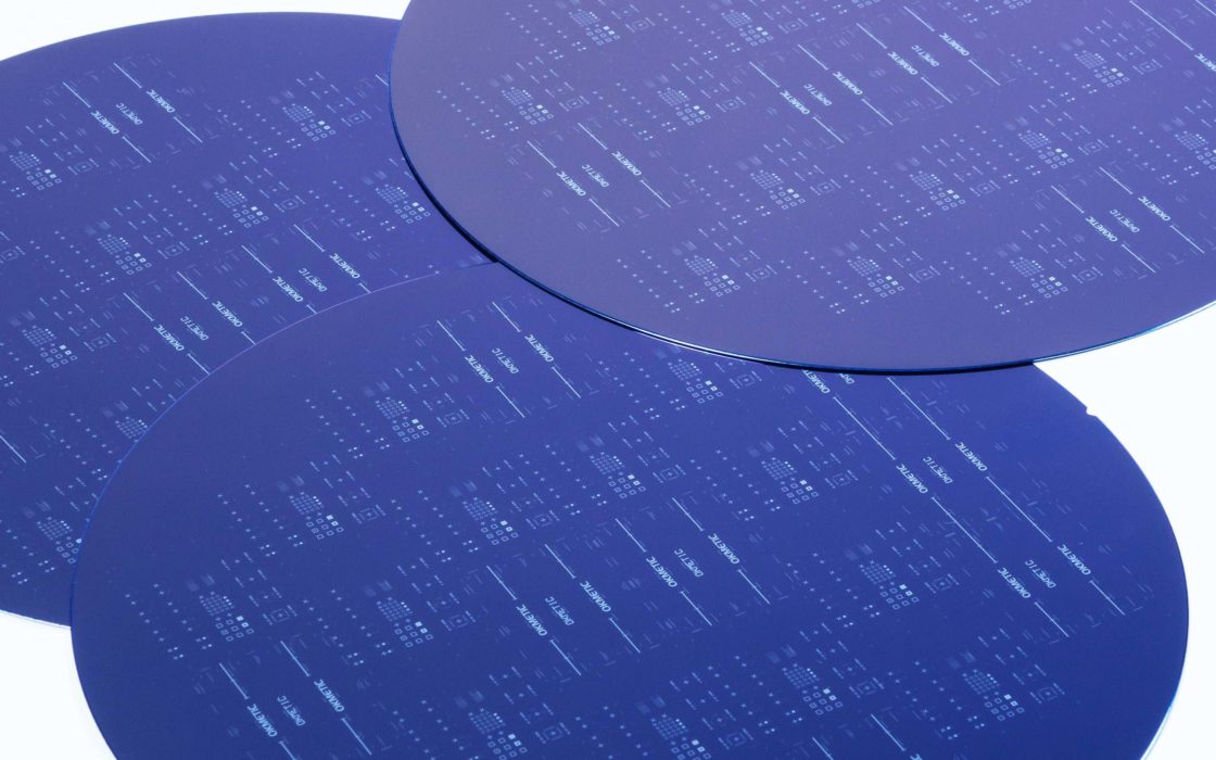
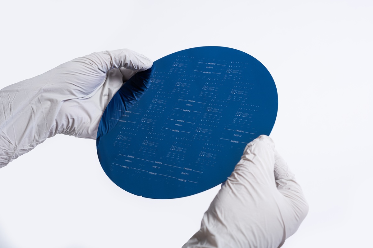
Okmetic Single Side Polished SSP wafers offer a perfect platform for surface MEMS, capping as well as RF and Power devices. In-house crystal growing and wide selection of wafer materials enable the manufacture of customized SSP wafer solutions. Available in 150-200 mm.
Crystal growing is one of Okmetic’s key competencies and it provides the foundation for the manufacture of customized SSP wafer solutions both in-house and in subcontracting. Our focus is on providing our customers with wide range of crystal materials and wafers for varied needs. Okmetic 200 mm SSP production capacity will see a significant increase starting in early 2025, following the expansion of its Vantaa site fab.
Wide range of crystal and wafer materials enable customized solutions for varied needs.
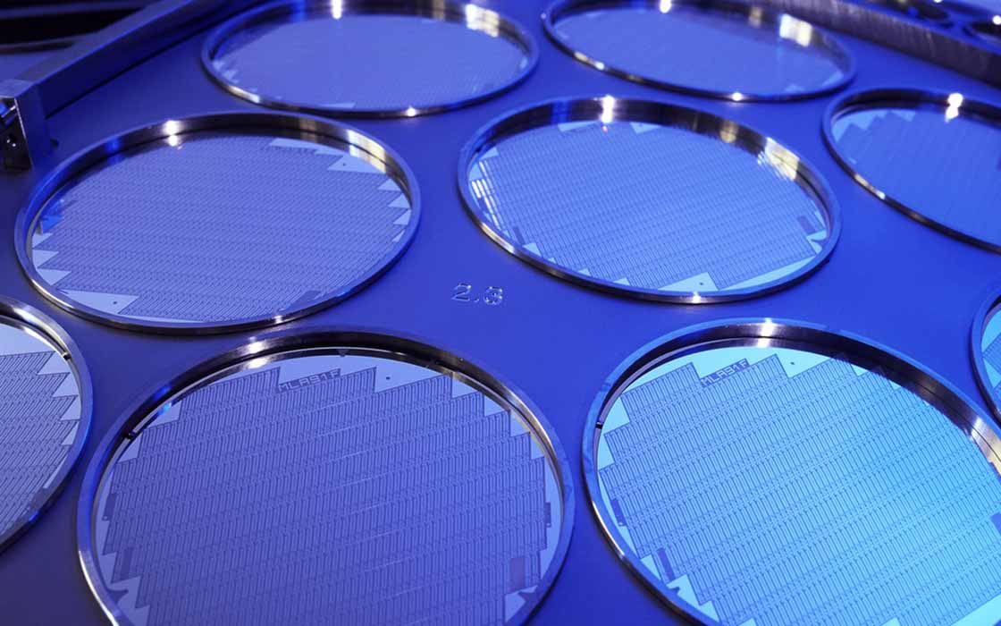
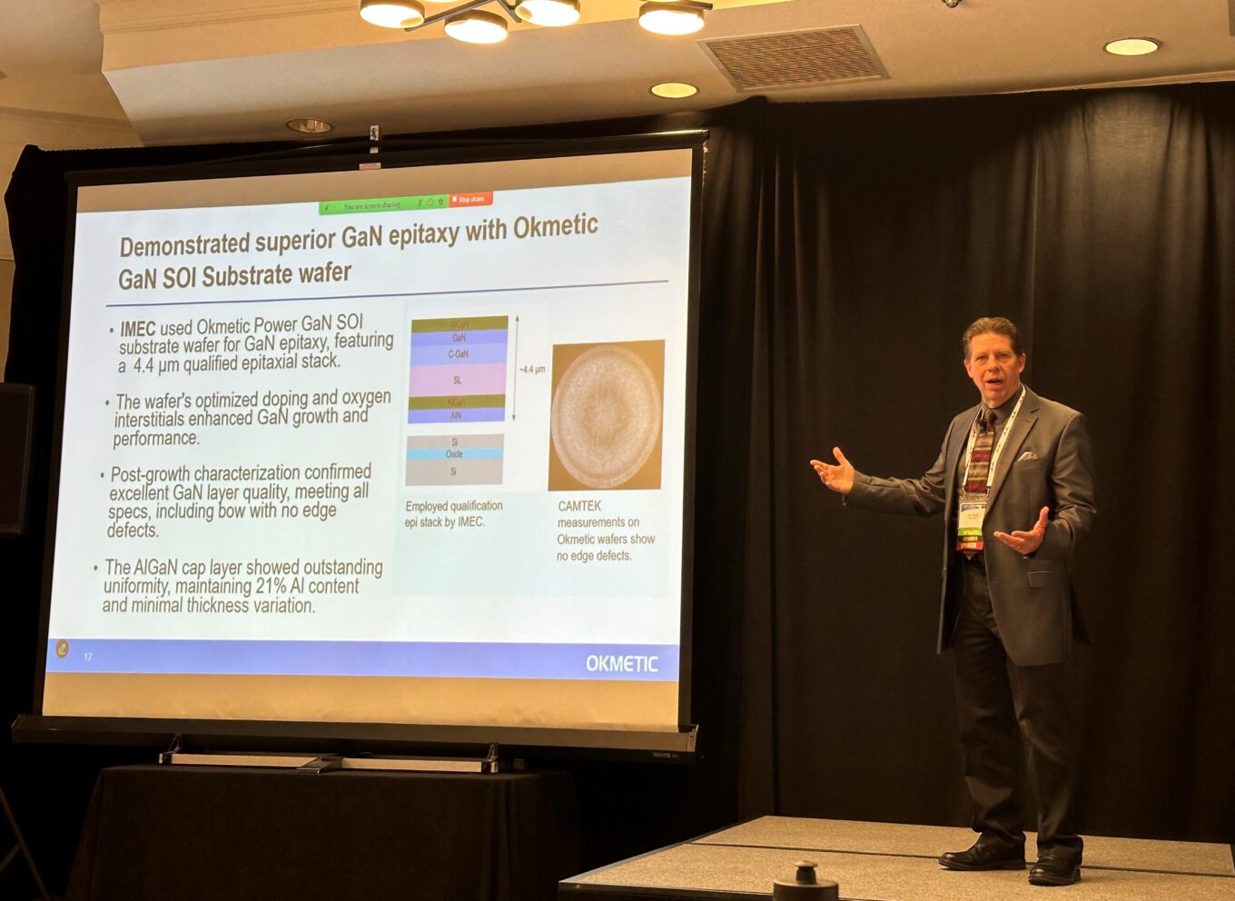
Our high-resistivity RFSi® wafer line includes SSP wafers for the needs of RF filters and devices and for GaN growth. Power wafer line includes SSP wafers tailored for the needs of discrete power devices and GaN growth. MEMS wafer line include SSP wafers optimized for the needs of surface MEMS and capping. These wafers are available with or without patterns. Many MEMS devices such as pressure sensors, accelerometers and gyroscopes are typically using SSP or DSP wafers as a platform, but the use of SOI wafers has long been on the increase for the sake of their cost-effectiveness.
Unparalleled SSP wafer capabilities
Okmetic’s in-house crystal growing creates unparalleled capabilities for the SSP wafers and thus customer’s processes. Okmetic Single Side Polished (SSP) wafers offered in 150 to 200 mm diameter are compatible even with the most demanding process lines due to our tight cleanliness and quality requirements. In addition, our SSP wafers have excellent thickness and flatness capabilities. Okmetic also supplies SSP wafers with non-standard thicknesses as certain specialty devices or applications require very thin SSP wafers or very thick SSP wafers as a platform. Thick wafers are suitable for example for GaN epi deposition.
Okmetic has wide selection of 150 to 200 mm SSP silicon wafers: Wafer dopants include antimony, arsenic, phosphorus, and boron. Crystal orientation can be <100>, <110>, <111> or off-oriented and thicknesses range from 400 to 1,150 µm and resistivities from <0.001 to >10,000 Ohm-cm. Backside finishing can be etched, polyback or LTO.
SSP wafer specifications
| Growth method | Cz, MCz, A-MCz® |
| Diameter | 200 mm, 150 mm |
| Crystal orientation | <100>, <110>,<111>, off-oriented |
| N type dopants | Antimony, Arsenic, Phosphorus, Red Phosphorus |
| P type dopants | Boron |
| Resistivity1 | Between <0.001 and >10,000 Ohm-cm |
| Thickness2 | 200 mm: 550 to 1,150 µm 150 mm: 400 to 1,150 µm |
| TTV3 | <1 μm |
| Backside finishing | Etched, Polyback, LTO |
2Other thicknesses possible with certain limitations.
3 Thickness limitations
Fully CMOS compatible wafer surface quality and cleanliness requirements
