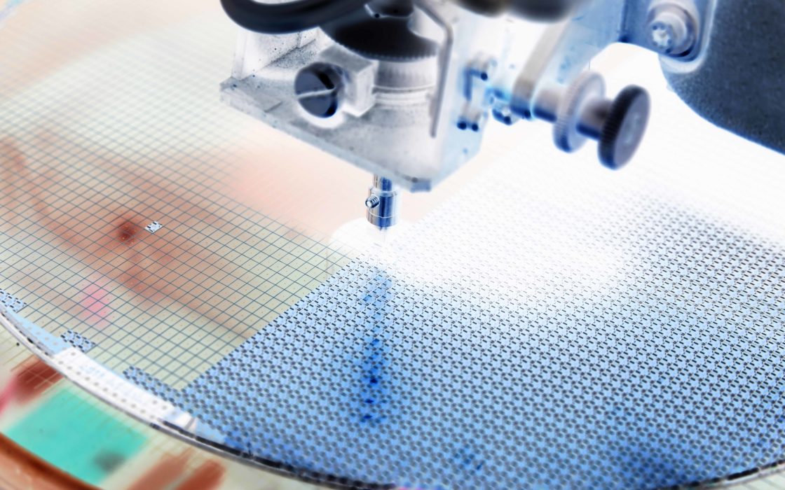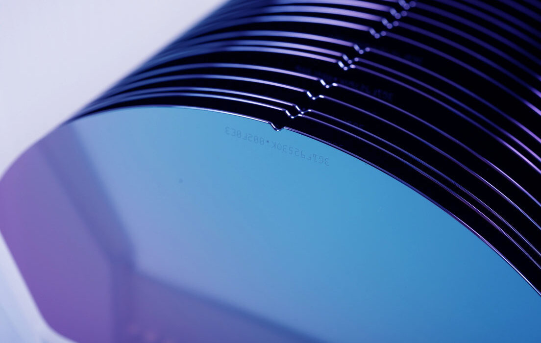
Low COP wafers (Si and SOI)
Okmetic Low COP silicon and SOI wafers feature minimal amount of critical size crystal-originated particles (COPs), positioning them as a cost-effective Float Zone alternative for advanced epi-free power IC devices. Okmetic ensures consistent Low COP wafer quality by utilizing Low COP A-MCz® crystal growth method.
Technological advancements and cost-efficiency requirements in the field of power semiconductors are fueling the need for thinner gate oxides and improved yield levels. Okmetic Low COP wafers address these requirements effectively as they feature minimal amount of COPs (crystal originated particles) near the wafer surface. COPs are known to impact gate oxide integrity (GOI) performance negatively, which is why their presence is a challenge for power devices utilizing medium to high resistivity wafers that lack inherent COP-free properties.
Okmetic Low COP wafers featuring minimal amount of COPs meet the power semiconductors’ need for thinner gate oxides and improved yield levels.
Okmetic Low COP wafers are manufactured using an optimized version of our signature Advanced Magnetic Czochralski (A-MCz®) crystal growth method, which removes the need for additional price-increasing annealing processes. Okmetic Low COP crystal capability is available for 200 mm Discrete Power Device and Power Management SOI wafers for resistivities of 1 Ohm-cm or above.
Enhanced GOI performance
The main challenge in controlling crystal-related surface defects in polished wafers lies in effectively managing the growth of agglomerated interstitial and vacancy-related defects during the crystal growth process. Vacancy-related defects, such as COPs and FPDs (Flow-Pattern Defects), can lead to near-surface issues during device manufacturing. Examples of these issues include compromised GOI (Gate Oxide Integrity) and current leakage in PN Junctions.
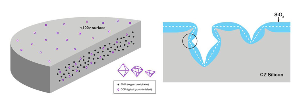
Okmetic Low COP wafers have minimal amount of critical-size crystal-originated particles (COPs), which ensures optimized GOI performance. The GOI performance can be further elevated by combining the low COP option with BMD optimization. Okmetic Low COP wafers are an ideal, cost-effective alternative to Float Zone wafers. They are particularly well-suited for advanced NPT/FS IGBT devices and for devices that use Okmetic Power Management SOI wafers, such as gate drivers and power ASICs.
Okmetic Low COP wafers are an ideal, cost-effective alternative to Float Zone wafers.
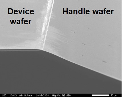
Superior surface quality without epitaxial deposition
Okmetic Low COP crystal growth method reduces total cost of ownership and removes the risk of thermal stress induced slip lines normally associated with traditional COP annealing processes.
The Low COP capability is available for 200 mm Discrete Power Device and Power Management SOI wafers utilizing boron or phosphorous doping, and having resistivity above 1 Ohm-cm. Otherwise, wafer customization options are similar to standard COP wafers. For example Power Management SOI wafers can also be Low COP and Terrace Free. Power Management SOI wafer is also available as Zero COP version with annealing process.
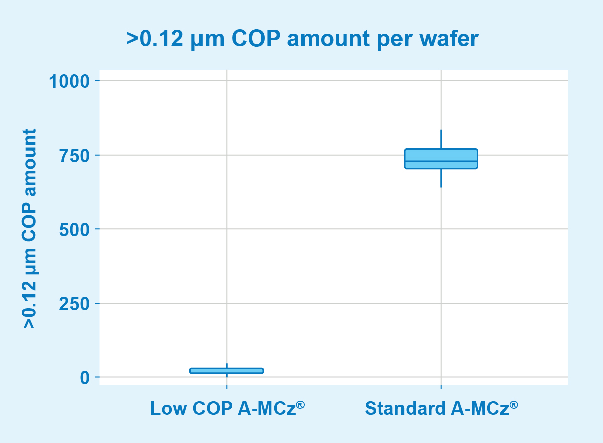
Comparison of 200 mm wafer COP amounts
| Standard A-MCz® | Low COP A-MCz® | |
| COP >0.10 μm | <2000 per wafer | <500 per wafer ( typically ~300 per wafer) |
| COP >0.12 μm | <1000 per wafer | <100 per wafer ( typically ~50 per wafer) |
Typical Low COP wafer specifications
| Growth method | Low COP A-MCz® |
| Diameter | 200 mm |
| Crystal orientation | <100> at the moment, <110> and <111> at later stage |
| N type dopants | Phosphorus |
| P type dopants | Boron |
| Resistivity1 | 1 to >1,500 Ohm-cm |
| Resistivity tolerance | Determined per price target and resistivity range |
| Radial resistivity gradient (RRG)2 | Typically below 8% |
| Oxygen concentration (Oi)3 | <4 to 14 ppma |
| Radial oxygen gradient (ROG)4 | Typically below 10% |
| Carbon concentration5 | <0.5 ppma |
| SSP wafer thickness6 | 550 to 1,150 μm |
| DSP wafer thickness6 | 380 to 1,150 μm |
| SSP backside treatment | Etched, Polyback, LTO |
| COP amount7 | COP >0.12 μm: <100pcs/wafer COP >0.10 μm: <500pcs/wafer |
2SEMI MF84, depends on the resistivity target and edge exclusion
3ASTM F121-831/SEMI MF1188-1107
4SEMI MF951, low Oi: ROG >20%
5ASTM F123-91, limited by measurement technology
6Other thicknesses possible with certain limitations.
7SP1 measurement
Fully CMOS compatible wafer surface quality and cleanliness requirements
Typical Low COP SOI wafer specifications
| Growth method | Low COP A-MCz® |
| Diameter | 200 mm |
| Crystal orientation | <100> at the moment, <110> and <111> at later stage |
| N type dopants | Phosphorus |
| P type dopants | Boron |
| Resistivity1 | 1 to >1,500 Ohm-cm |
| Resistivity tolerance | Determined per price target and resistivity range |
| Oxygen concentration (Oi)2 | <4 to 14 ppma |
| Device layer thickness3 | 1 μm to >200 μm (±0.1 µm) |
| Buried oxide layer thickness4 | 0.3 μm to >5 μm |
| Handle wafer thickness5 | 300 μm to 950 μm (±3-5 µm) |
| Back surface | Polished, etched, oxide or without oxide |
| COP amount6 | COP >0.10 μm: <500 per wafer COP >0.12 μm: <100 per wafer Zero COP SOI available with annealing process |
| Terrace area7 | Standard or Terrace Free (depends on wafer size and thickness) |
range varies by dopant and orientation.
2ASTM F121-831/SEMI MF1188-1107
3Other thicknesses possible with certain limitations.
4Type: thermal oxide. Typically 0.5 μm to 2 μm, thicker BOX possible with certain limitations.
5 200 mm: typically 725 μm ±3 µm tolerance for demanding devices
6SP1 measurement
7 Terrace Free available in 200mm and 725 μm thickness
Fully CMOS compatible wafer surface quality and cleanliness requirements