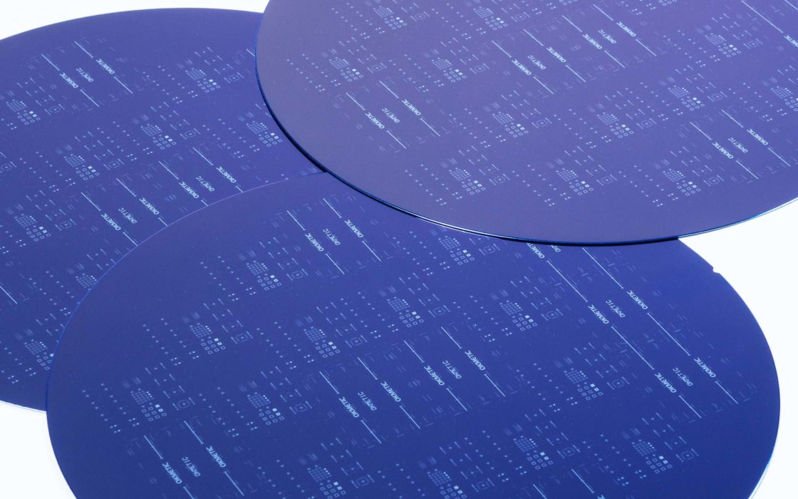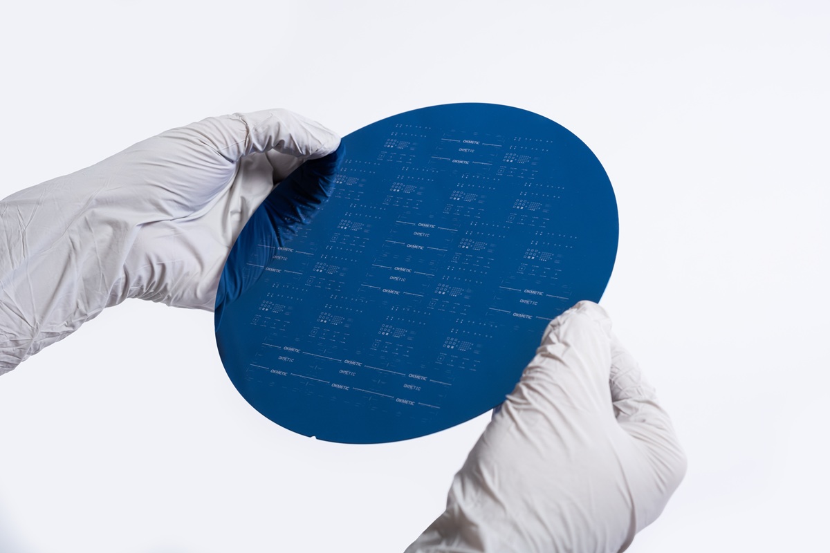
Selecting the ideal wafer for MEMS devices: Balancing cost, performance, and manufacturing efficiency
In the rapidly evolving world of MEMS manufacturing, choosing the right substrate is critical. As manufacturers focus on cost-efficiency, performance, and miniaturization, understanding substrate differences is key to optimizing device production.
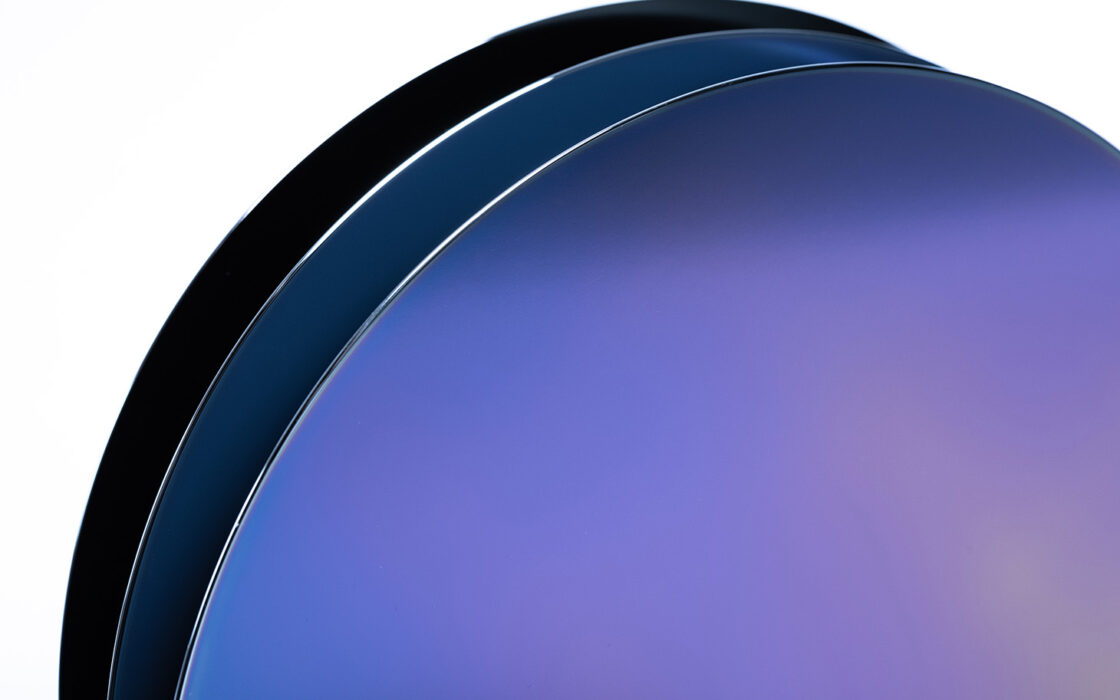
When choosing between Single Side Polished (SSP), Double Side Polished (DSP), Bonded Silicon-On-Insulator (SOI), Enhanced SOI (E-SOI®), and Cavity Silicon-On-Insulator (C-SOI®) wafers for your MEMS device, it’s vital to evaluate the specific demands of your application and manufacturing process, device performance, and cost structure. Each wafer type presents unique advantages that impact both performance and cost-effectiveness.
- Application and manufacturing compatibility: SSP wafers are well-suited for bulk micromachining and basic MEMS structures. DSP wafers are ideal for applications requiring high precision or dual-sided processing. Bonded SOI wafers excel in high-performance applications where a precise etch stop or electrical isolation is critical, and devices require electrical integration. E-SOI® wafers are best suited for applications requiring extremely tight device layer uniformity. C-SOI® wafers are perfect for complex designs and can enable cutting down process steps at the device line.
- Device performance and reliability: For devices that demand high performance and low power consumption, and effective thermal management, Bonded SOI wafers are an optimal choice. If your design includes cavities or requires high precision, C-SOI® wafers offer distinct advantages.
- Cost considerations: SSP wafers are typically the most budget-friendly option, while DSP wafers provide improved precision at a slightly higher cost. However, prices for both can vary based on specifications and order quantities. Bonded SOI, Enhanced SOI (E-SOI®), and Cavity SOI (C-SOI®) wafers, though more expensive, offer significant cost advantages by streamlining device processing and enhancing performance for demanding devices, ultimately reducing total cost of ownership through optimized efficiency.
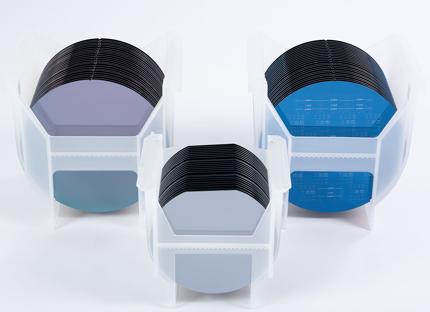
SSP and DSP wafers: High quality and precision for MEMS manufacturing
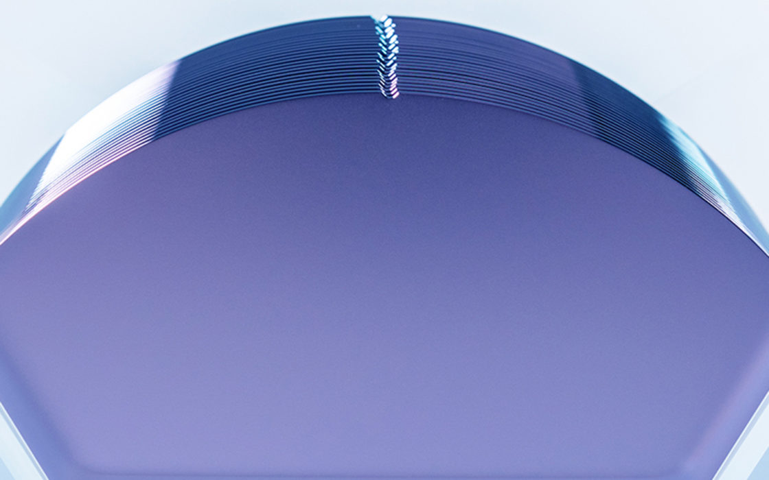
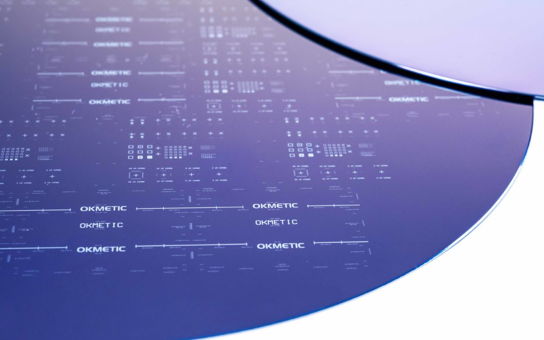
Okmetic MEMS SSP and DSP wafers are available with or without patterns and they meet stringent cleanliness and quality standards. In-house crystal growing and wafering provides unmatched capabilities for SSP wafers, ensuring compatibility with demanding process lines. These SSP wafers offer excellent thickness and flatness capabilities and SFQR values. Their superior surface quality makes them ideal for MEMS device manufacturing, where precision and reliability are crucial.
Our DSP wafers provide outstanding thickness uniformity and orientation accuracy, making them perfect for MEMS devices. Their superior quality supports applications requiring double-sided lithography, wafer bonding, or precise alignment. Widely used as cap wafers, Okmetic DSP wafers excel in bonding strength and hermetic sealing with various bonding techniques.
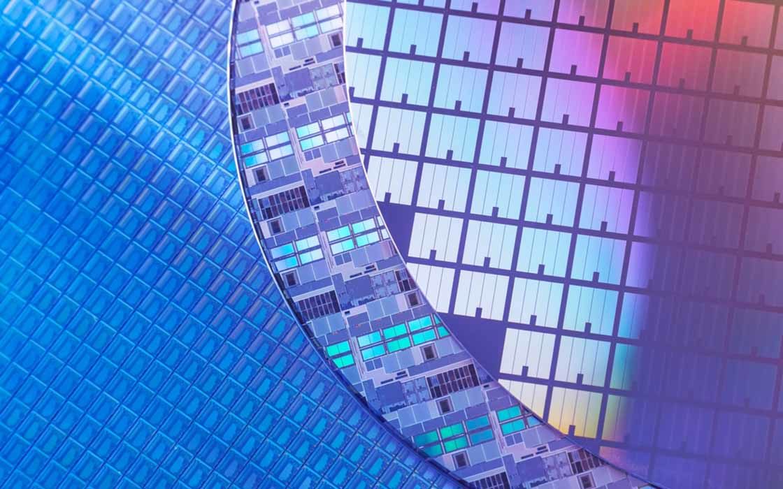
SOI wafers enable cost-effective MEMS manufacturing, enhance yield, and simplify processing
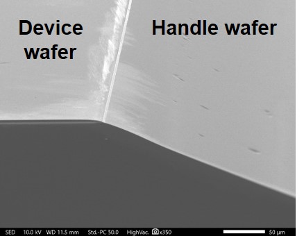
Okmetic SOI wafers are manufactured by bonding two silicon wafers with an insulating oxide layer between them. The top device layer houses sensing elements and integrated circuits (ICs), while the bottom handle wafer supports the structure and can aid in sealing or sensing. The buried oxide layer is an excellent electric insulating layer, and it also forms an effective etch-stop in device manufacturing. It can also act as a sacrificial layer when manufacturing more complex devices. This design reduces parasitic capacitance, ideal for high-performance applications.
Okmetic’s advanced in-house bonding and patterning processes ensure that Bonded SOI, E-SOI® and C-SOI® wafers comply with the highest standards of quality and precision required for MEMS production. These SOI wafers offer notable advantages, such as cost-efficiency, reduced chip size, and improved performance. C-SOI® wafers provide enhanced design flexibility and simplify processing, thanks to their integrated cavities. The layered structure of Bonded SOI, E-SOI® and C-SOI® wafers enhances electrical isolation, thermal management, and overall design adaptability, making them well-suited for sophisticated and advanced MEMS applications.
Cost-efficiency and size reduction
Bonded SOI, E-SOI® and C-SOI® wafers deliver substantial cost-efficiency in MEMS manufacturing, reducing chip sizes to as little as one-third of traditional designs. These wafer types feature a buried oxide layer that simplifies processing, enhances electrical isolation, and boosts yield and reliability. Additionally, C-SOI® wafers with pre-etched cavities streamline the manufacture of complex MEMS devices. The ability to incorporate cavities within the wafer also enables more sophisticated device designs, improving both functionality and performance.
Terrace Free SOI wafer capability available for Bonded SOI and E-SOI® wafers further add cost-efficiency through increased usable wafer area, reduced edge exclusion as well as improved yield and handling enabling also easier stacking of the silicon wafers.
Optimized electrical performance and precision
The layered structure of Bonded SOI wafers enhances MEMS performance and precision through key features like the buried oxide layer, which provides excellent electrical isolation. This reduces parasitic effects and leakage currents, improving device efficiency and performance. The insulating layer minimizes crosstalk between microstructures and circuits, further enhancing MEMS accuracy. These features, along with reduced resistance and parasitic capacitance, support faster response times and lower power consumption, making Bonded SOI wafers ideal for high-performance, power-sensitive applications.
Enhanced thermal and radiation resistance
Bonded SOI wafers with a buried oxide (BOX) layer enhance stability, sensitivity, and overall performance in MEMS applications, with effective thermal management being a lesser-known benefit. In inertial and pressure sensors, the BOX layer reduces thermal crosstalk and drift, ensuring precision in fluctuating temperatures. Infrared sensors and microbolometers benefit from this thermal isolation, improving sensitivity for thermal imaging and remote sensing. Thermal actuators use the BOX layer for efficient heat concentration, enhancing responsiveness, while resonators and oscillators rely on this insulation to stabilize frequency, crucial for telecommunications and navigation systems.
The insulating layer also offers enhanced radiation resistance, making MEMS devices more reliable in high-radiation environments, such as space applications or radiation monitoring. This combination of thermal and radiation protection is crucial for maintaining the performance and longevity of MEMS devices in challenging conditions.
Precision thickness control and design flexibility
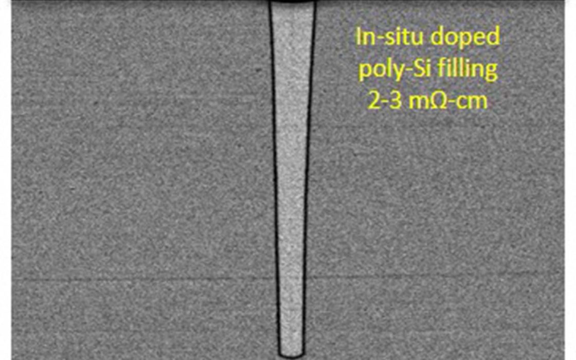
Bonded SOI, E-SOI® and C-SOI® wafers all offer precise control over the thickness of silicon and oxide layers, enabling the development of MEMS devices with accurate and consistent dimensions. C-SOI® wafers, in particular, provide greater flexibility for more advanced designs due to their pre-etched cavities. This allows manufacturers to implement advanced designs while maintaining high performance and reliability. Bonded SOI, E-SOI® and C-SOI® wafers support complex circuit designs and advanced manufacturing techniques, ultimately improving device functionality and overall system integration. With nearly 20 years of expertise in Cavity SOI, Okmetic offers highly customized and advanced C-SOI® wafers. These wafers can include solutions such as double device layers, patterned device layers, polyfilled TSVs, and highly uniform device layers.
Okmetic’s MEMS wafer line consist of the following products:
Contact us
Request a quote or product details
Application areas
- Inertial sensors / accelerometers, gyroscopes and IMUs
- Pressure sensors
- MEMS based microfluidic devices, bio MEMS and flow sensors
- Transducers and actuators
- Silicon speakers
- Silicon photonics, optical MEMS devices (MOEMS)
- MEMS oscillators and silicon timing devices
- Resonators
- Ultrasonic transducers like PMUT and CMUT
- IC and MEMS process integrations
- Mechanical parts
- CAP wafers
- And more..