MEMS SSP and DSP wafers
Okmetic MEMS optimized Single Side Polished SSP and Double Side Polished DSP wafers offer a perfect platform for surface micromachining and capping. In-house crystal growing and wide selection of wafer properties enable the manufacture of customized SSP wafer solutions. Our MEMS SSP and DSP wafers are available with or without patterns and in 150-200 mm.
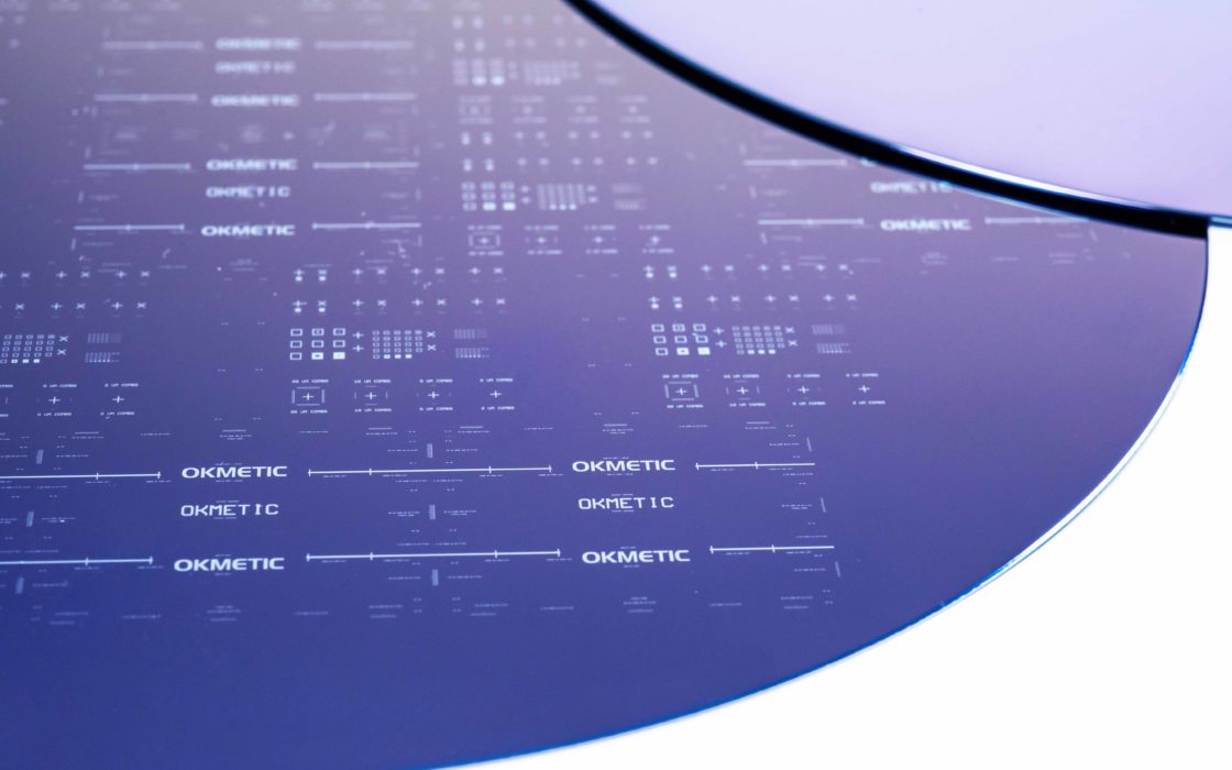
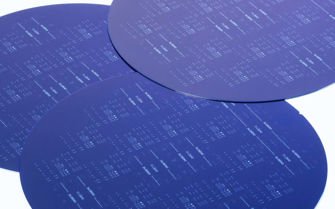
Okmetic MEMS optimized SSP and DSP wafers are available in high-volume CMOS-compatible production. The wafer parameters are fully customizable to meet device manufacturers’ process needs, enabling high-precision sensing elements with stable quality and efficient processing. Okmetic also has in-house capability for built-in patterns. Read more about our high-quality patterned wafers, which enable more streamlined device manufacture.
MEMS SSP and DSP wafers are a good match for surface MEMS, capping and bulk micromachining. They can also be used as part of the bonded MEMS structure.
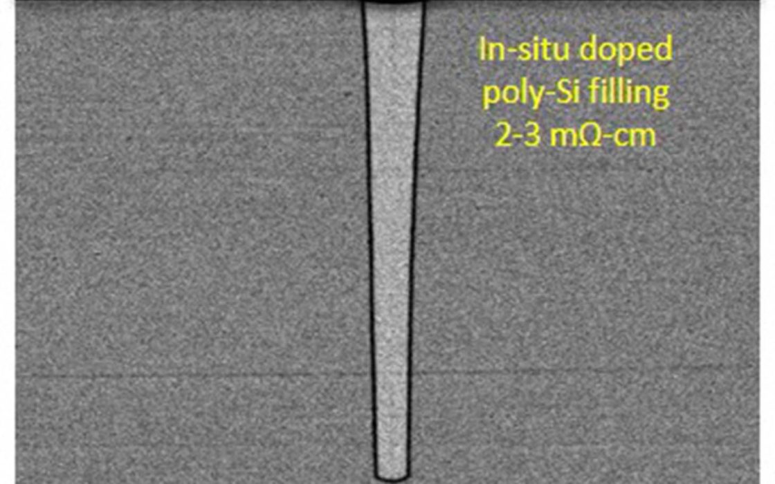
MEMS SSP and DSP wafers are a good match for surface MEMS, capping and bulk micromachining. They can also be used as part of the bonded MEMS structure. SSP wafers are often used in applications such as pressure sensors, accelerometers, microfluidic devices, and micromirrors among others. DSP wafers are used more often e.g. in advanced inertial sensors (gyroscopes, high-performance accelerometers), resonators and optical MEMS. Also, MEMS devices that incorporate TSVs (Through-Silicon-Vias) for electrical connections through the wafer use DSP wafers to enable the precise etching and filling of vias. Read more about our TSV wafers.
For cutting-edge device designs or enhanced cost-efficiency, explore our Bonded SOI wafer solutions.
SSP wafers compatible with demanding process lines
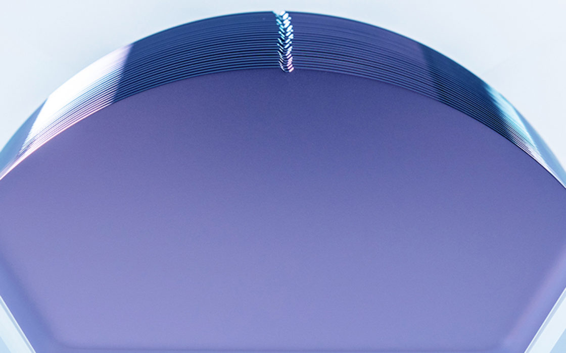
Okmetic in-house crystal growing and wafering provides unmatched capabilities for SSP wafers, ensuring compatibility with demanding process lines. These SSP wafers meet stringent cleanliness and quality standards, offering excellent thickness and flatness capabilities.
DSP wafers with excellent thickness uniformity and orientation accuracy
Okmetic Double Side Polished (DSP) wafers offer exceptional thickness uniformity, orientation accuracy, and crystal quality, making them an ideal platform for MEMS devices. Okmetic DSP wafers, known for their superior quality, are ideally suited for MEMS device manufacturing that requires double-sided lithography, wafer bonding, or precise alignment marks and structures on both surfaces. Okmetic DSP wafers are widely used as cap wafers in MEMS devices, providing excellent bonding strength and hermetic sealing when used with fusion, anodic, eutectic, and glass frit bonding techniques.
Okmetic DSP wafers ensure high precision, stable quality, and efficient processing.
Optimized for bulk micromachining and alkali etching (e.g., KOH, TMAH), our DSP wafers ensure high precision, stable quality, and efficient processing. Additionally, our thin DSP wafers enable faster processing, offering cost and quality advantages. The wide selection of wafer parameters allows for highly customized solutions, ensuring precise alignment and minimal distortion during critical MEMS fabrication processes.
Wide selection of SSP and DSP wafer parameters
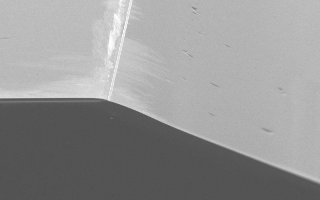
Okmetic has wide selection of 150 to 200 mm MEMS optimized SSP and DSP silicon wafers: Wafer dopants include antimony, arsenic, phosphorus, and boron. Crystal orientation can be <100>, <110>, <111> or off-oriented and thicknesses range from 380 to 1,150 µm. The wafers have excellent thickness uniformity and flatness. MEMS SSP and DSP wafer resistivities range from <0.001 to >7,000 Ohm-cm. Backside finishing include etched, polyback or LTO. DSP wafers can also have backside alignment marks thanks to Okmetic in-house patterning capability. Edge shape can be optimized to meet the requirements of customer process.
General SSP and DSP wafer specifications for MEMS devices
| wth method | Cz, MCz, A-MCz® |
| Diameter | 200 mm, 150 mm |
| Crystal orientation | <100>, <110>, <111>, off-oriented |
| Orientation accuracy1 | ±0.2° |
| N type dopants | Antimony, Arsenic, Phosphorus, Red Phosphorus |
| P type dopants | Boron |
| Resistivity2 | Between <0.001 and >7,000 Ohm-cm |
| SSP wafer thickness3 | 200 mm: 550 to 1,150 μm 150 mm: 400 to 1,150 μm |
| SSP TTV4 | <1 μm |
| Backside finishing | SSP: Etched, Polyback, LTO DSP: Backside alignment mark |
| DSP wafer thickness3 | 200 mm: 380 to 1,150 μm 150 mm: 380 to >1,150 μm |
| DSP thickness tolerance5 | (±5 µm) |
| DSP TTV4 | ≤0.7 μm |
| Edge | 200 mm: polished4, etched 150 mm: etched |
2 Over 1,500 Ohm-cm is possible with P-type boron doping. Resistivity range varies by dopant and orientation. Engineered Ultra High Resistivity wafers for >10,000 Ohm-cm resistivity.
3Other thicknesses possible with certain limitations.
4 Thickness limitations
5 ±3 µm for demanding devices
Fully CMOS compatible wafer surface quality and cleanliness requirements