MEMS wafer line
Okmetic MEMS wafer line provides an optimal platform for the manufacture of various MEMS and sensor devices. Our MEMS and sensor device optimized silicon wafer solutions improve device performance, reduce Total Cost of Ownership and enable more refined designs.
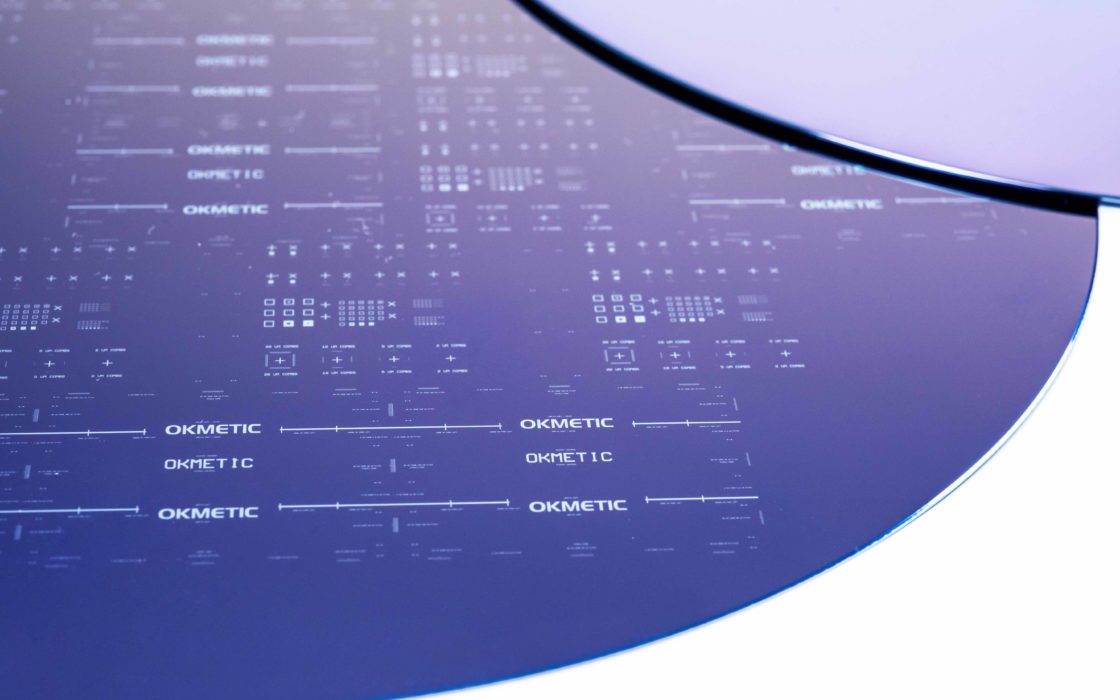
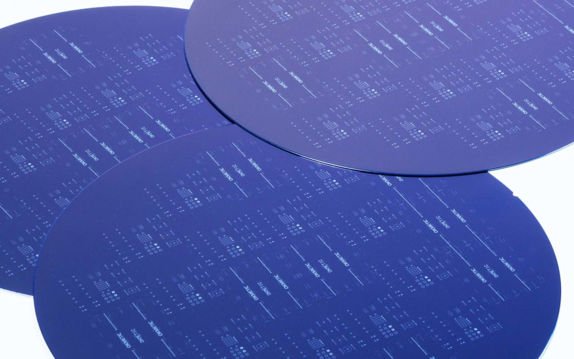
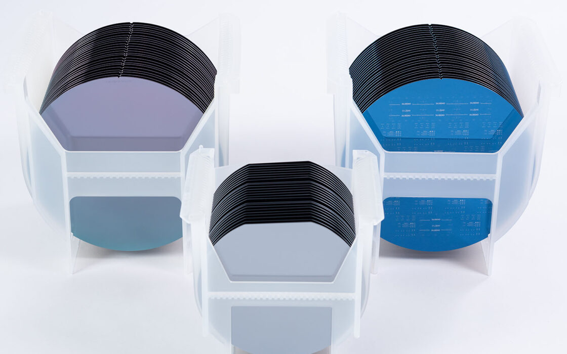
Okmetic is the leading supplier of advanced silicon wafers for the MEMS and sensor market, with a dedicated focus on delivering customized wafer solutions for the MEMS industry since its foundation. Our wide range of MEMS optimized silicon wafers provide an optimal platform for the manufacture of various MEMS devices.
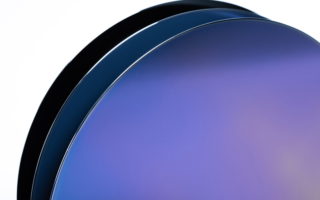
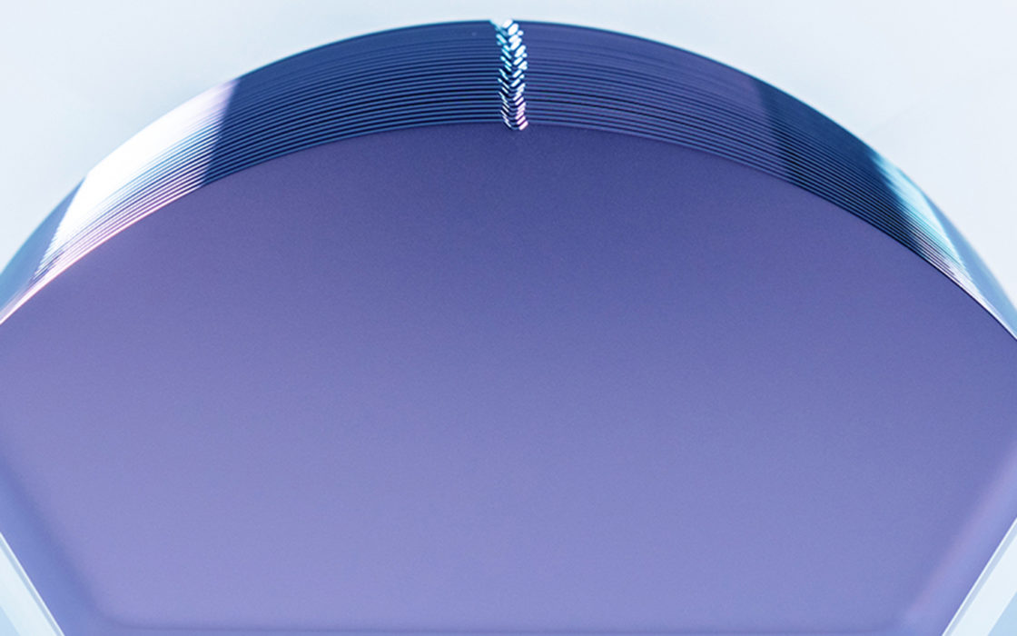
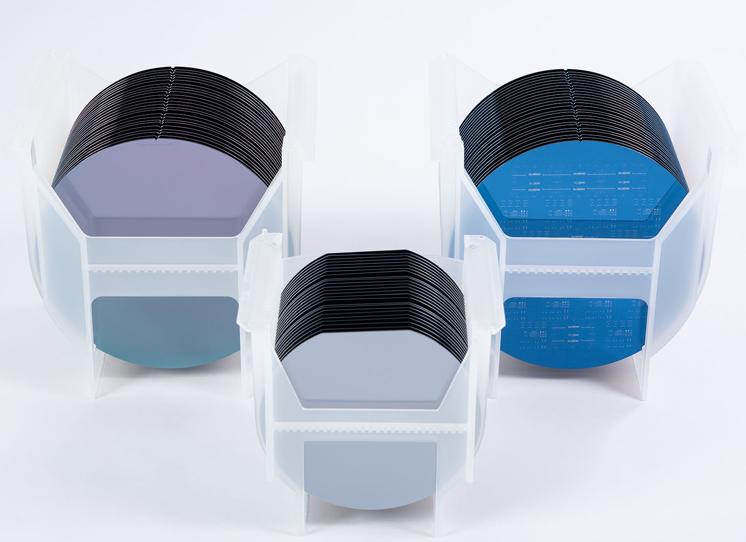
SSP and DSP wafers with or without patterns are often used as part of the bonded MEMS structure or as a cap wafer. However, the use of Silicon-On-Insulator (SOI) wafers has long been on the increase for the sake of their cost-effectiveness. With BSOI or C-SOI® (Cavity SOI) wafer the chip size can be reduced easily to one third. C-SOI® also reduces the processing steps at the customer site reducing total cost of ownership.
Okmetic is the leading supplier of advanced silicon wafers for the MEMS and sensor market, with a dedicated focus on delivering customized wafer solutions
Okmetic SOI wafers are manufactured by bonding two silicon wafers together and leaving an insulating oxide layer between them. The top device layer is typically used for sensing elements, while the buried oxide layer serves as an electrical insulator, etch-stop, or sacrificial layer. The bottom handle wafer supports the structure and can also aid in sealing or functioning as part of the sensing element.
Comprehensive line of MEMS wafers
Okmetic has comprehensive MEMS wafer line available in 150-200 mm. Resistivity, crystal orientation, oxygen content, thickness, possible oxide layer and wafer edge can be customized to match your product or package needs. Our sales and technical support are happy to help find an optimal solution, customized for your needs.
Okmetic’s MEMS wafer line consist of the following products:
Read article how to select ideal wafer for your MEMS device: balancing cost, performance and manufacturing efficiency.
General SSP and DSP wafer specifications for MEMS devices
| Growth method | Cz, MCz, A-MCz® |
| Diameter | 200 mm, 150 mm |
| Crystal orientation | <100>, <110>, <111>, off-oriented |
| Orientation accuracy1 | ±0.2° |
| N type dopants | Antimony, Arsenic, Phosphorus, Red Phosphorus |
| P type dopants | Boron |
| Resistivity2 | Between <0.001 and >7,000 Ohm-cm |
| SSP wafer thickness3 | 200 mm: 550 to 1,150 μm 150 mm: 400 to 1,150 μm |
| SSP TTV4 | <1 μm |
| Backside finishing | SSP: Etched, Polyback, LTO DSP: Backside alignment mark |
| DSP wafer thickness3 | 200 mm: 380 to 1,150 μm 150 mm: 380 to >1,150 μm |
| DSP thickness tolerance5 | (±5 µm) |
| DSP TTV4 | ≤0.7 μm |
| Edge | 200 mm: polished4, etched 150 mm: etched |
2 Over 1,500 Ohm-cm is possible with P-type boron doping. Resistivity range varies by dopant and orientation. Engineered Ultra High Resistivity wafers for >10,000 Ohm-cm resistivity.
3Other thicknesses possible with certain limitations.
4 Thickness limitations
5 ±3 µm for demanding devices
Fully CMOS compatible wafer surface quality and cleanliness requirements
General SOI specifications
| Growth method | Cz, MCz, A-MCz® |
| Diameter | 200 mm, 150 mm |
| Crystal orientation | <100>, <110>,<111> |
| N type dopants | Antimony, Phosphorus |
| P type dopants | Boron |
| Resistivity1 | Between <0.001 and >7,000 Ohm-cm |
| Device layer thickness2 | From 1 μm to >200 μm Tolerance ±0.5 μm (standard BSOI), ±0.3 μm (0.3 SOI), ±0.1 μm (E-SOI®), ±0.5 μm or lower (C-SOI®) |
| Buried oxide layer thickness3* | From 0.3 μm to >5 μm Type: Thermal oxide |
| Handle wafer thickness4 | 300 μm to 950 μm (±3-5 µm) |
| Back surface | Polished or etched |
| Terrace area | Standard or Terrace Free (Available for 200 mm BSOI, E-SOI® and Power Management SOI) |
2Other thicknesses possible with certain limitations. 150 mm E-SOI® tolerance ±0.2 µm.
3Type: thermal oxide. Typically 0.5 μm to 2 μm, >5 μm BOX possible with certain limitations.
4200 mm: typically 500-725 μm. 150 mm: typically 380-675 μm. ±3 µm tolerance for demanding devices. Handle thickness range is narrower for C-SOI® wafers.
*Possibility also for two device and buried oxide layers with different thicknesses.
Fully CMOS compatible wafer surface quality and cleanliness requirements
Contact us
Request a quote or product details
Application areas
- Inertial sensors / accelerometers, gyroscopes and IMUs
- Pressure sensors
- MEMS based microfluidic devices, bio MEMS and flow sensors
- Transducers and actuators
- Silicon speakers
- Silicon photonics, optical MEMS devices (MOEMS)
- MEMS oscillators and silicon timing devices
- Resonators
- Ultrasonic transducers like PMUT and CMUT
- IC and MEMS process integrations
- Mechanical parts
- CAP wafers