Power wafer line provides optimized substrate solutions for the growing market
Power electronics market continues to grow due to electrification, increased demand for renewable energy sources and higher efficiency standards. In 2022, the total power market was worth over 20 BUSD, and the Compound Annual Growth Rate (CAGR) is anticipated to be 4-8% for the next few years. Increasing demand for power electronic devices in automotive, consumer, industrial and mobility markets will drive up the overall need for wafers.
Okmetic Power wafer line provides an optimal platform for the manufacture of various power devices. Our power device optimized wafer solutions improve power device performance, reduce Total Cost of Ownership and enable more refined designs.
Power Management SOI wafers have benefits over bulk silicon wafers
Power Management SOI wafers provide a cost-effective substrate choice for power management devices since their inherent isolation capability pushes towards monolithic integration reducing the die size. The device and buried oxide layer specification flexibility helps establish high freedom of design to streamline the chip development process.
Power Management SOI wafers combine customizable resistivity, tight resistivity control, low and controlled Oi levels and zero BMDs. They are also available as Terrace Free version in 200 mm wafer size. Power Management SOI wafers are mainly used in Gate drivers for power devices, Battery and Power Management ICs, Intelligent Power Modules, and other Smart Power devices using advanced BCD or BiCMOS processes.
Read more: Power Management SOI wafers | Okmetic
Power GaN Substrate wafers provide advanced stress management
Fully customizable gallium nitride (GaN) silicon substrate wafers with advanced stress management provide an enhanced platform for up to 1200 V lateral GaN power devices. All parameters including wafer thickness, crystal orientation and oxygen levels can be customized to enhance customer’s GaN epitaxy process efficiency and end product capability.
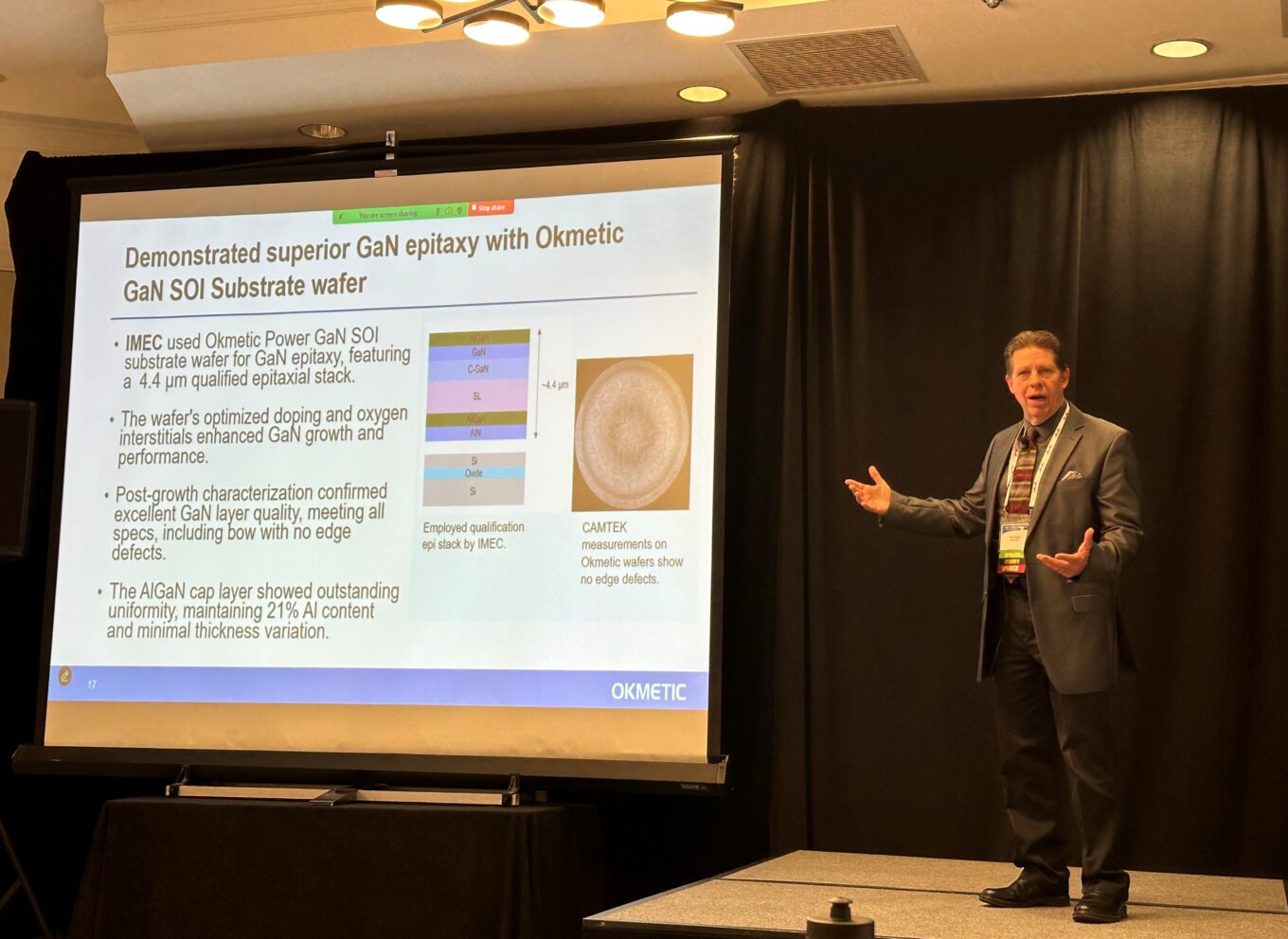
Further benefits can be gained through GaN growth on SOI wafers. The layered structure of the SOI substrate enables monolithic integration increasing device performance and power efficiency, reduces dislocations and allows the use of thinner buffer layers.
Read more: Power GaN Substrate wafers (Si and SOI) | Okmetic
Discrete Power Device wafers are fully customizable
Okmetic has decades expertise in Discrete Power Device wafers that offer customizable resistivity between <0.001 and >350 Ohm-cm, tight resistivity control, low and controlled Oi level and low defect density. Discrete Power Device wafers are BMD, dislocation and slip free. In addition, the COP levels can be controlled if needed. Discrete Power Device wafers are widely used e.g., in power MOSFETs, IGBTs, Schottky and power diodes, power BJTs, thyristors as well as in CMOS and BiCMOS manufactured devices.
Read more: Discrete Power Device wafers | Okmetic


