Power GaN Silicon and SOI Substrate wafers: Advancing high-performance GaN growth
As GaN technology drives advancements in high-performance power applications, substrate optimization is essential for successful GaN growth. Okmetic Power GaN-optimized Silicon (Si) and Silicon-on-Insulator (SOI) wafers are engineered to provide the robustness needed during GaN epitaxy. These wafers deliver enhanced stability, reduced wafer bowing, and superior electrical characteristics, making them the ideal platform for high-performance GaN-based devices.
Polished silicon wafers are a mainstream solution for GaN growth due to their cost-effectiveness and good availability compared to alternatives like Silicon Carbide (SiC) and Sapphire. However, SOI wafers are gaining increasing attention for their superior device isolation, reduced parasitic capacitance, and improved thermal stability—key benefits for power devices. While GaN-on-Si and GaN-on-SiC growth technologies remain the established choices for high-power applications, bonded SOI structures are emerging as a promising alternative. These structures offer a unique advantage in device integration, as GaN growth technologies evolve, enabling more efficient and scalable device manufacturing. Recent collaboration with Interuniversity Microelectronics Centre (IMEC) has yielded very promising results, particularly highlighting the potential of SOI wafers for GaN growth.
Silicon Substrate wafers designed for GaN growth
Okmetic Power GaN Substrate wafers, available as Single Side Polished and Double Side Polished, are specifically engineered to meet the demanding requirements of GaN epitaxial processing. These wafers are designed to reduce wafer bow and warpage while enhancing durability. The robustness of our Power GaN Substrates is supported by our Advanced Magnetic Czochralski (A-MCz®) crystal growth process, which allows for ultra-high dopant concentration and optimized oxygen interstitial (Oi) levels. This process not only fortifies the lattice structure but also enables precise orientation control, ensuring superior stress management.
Designed for flexibility, Okmetic Power GaN Substrates can be fully customized to meet the specific needs of a wide range of GaN applications. Available in <111> orientation, these substrates support high-voltage GaN HEMT devices (beyond 650V) and high-power LEDs. For applications requiring enhanced durability, thicknesses up to >1,150 µm are available to further reduce bowing and warpage. Optional poly and LTO back surfaces provide additional stress resilience.
IMEC validates GaN SOI Substrate wafers for high-quality GaN epitaxy
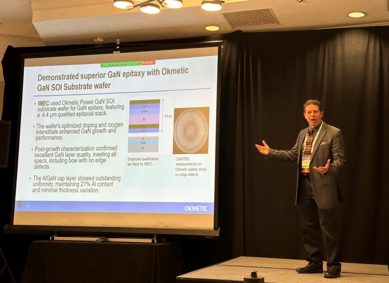
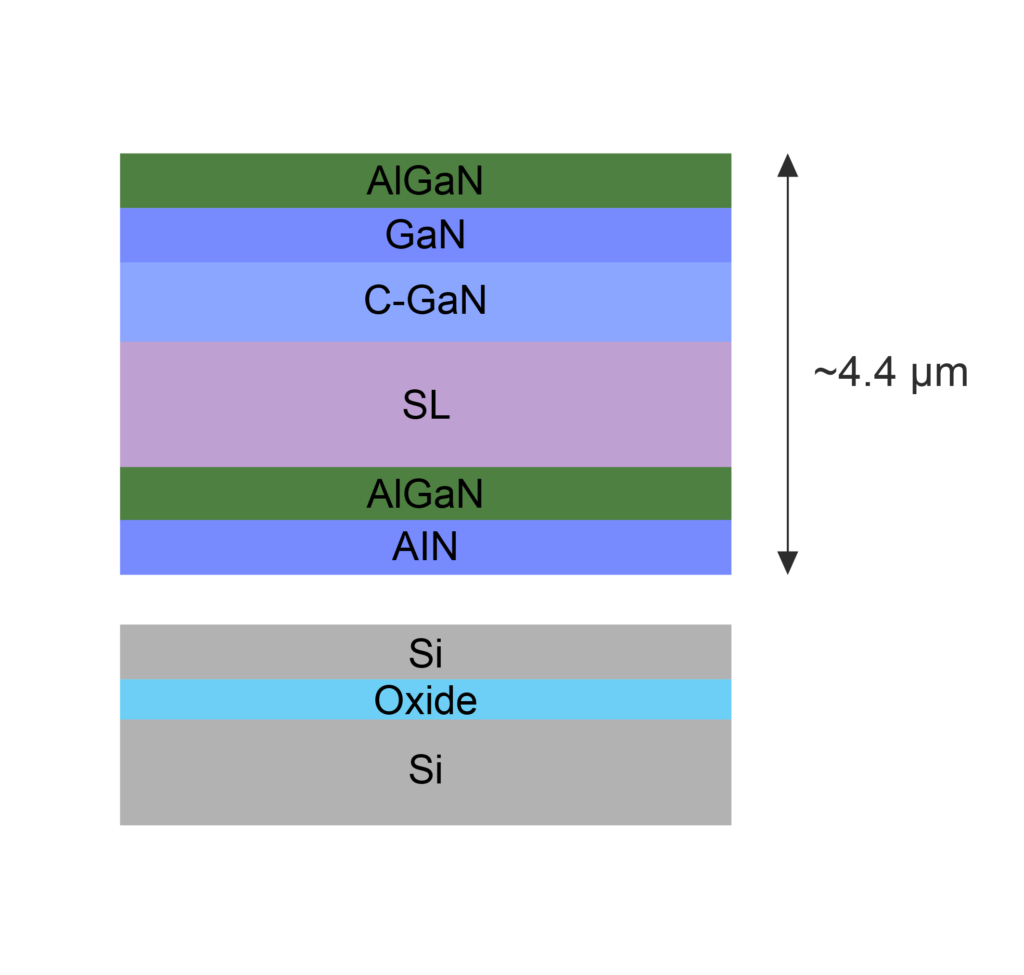
A recent study by IMEC evaluated Okmetic’s GaN-optimized and non-optimized SOI wafers, comparing their effects on GaN growth, wafer bowing, and stability. IMEC successfully grew a 4.4 µm GaN-epi-stack on Okmetic wafers, with the GaN-optimized SOI wafers showing superior GaN layer uniformity, reduced wafer bowing, and enhanced electrical performance in post-growth studies. IMEC electrical performance testing, including buffer breakdown, hall measurements, and dispersion analyses, demonstrates that Okmetic Power GaN SOI substrate wafers deliver comparable performance to industry-leading materials, which served as a reference in the study.
The study confirms the Power GaN SOI Substrate wafers’ stability and suitability for high-power applications. They offer both high electrical reliability and exceptional performance under high-temperature conditions, which are critical for long-term durability and efficiency in demanding applications.
SOI Substrate wafer specifications
Both GaN-optimized and non-optimized SOI wafers had identical specifications for the device and buried oxide layers, as well as for handle layer thickness. Both also utilized a <111> crystal orientation, known for enhancing wafer durability. The key distinction between the two types of wafers lies in the GaN-optimized SOI wafers, which feature higher doping and oxygen interstitial (Oi) concentrations in the handle layer. This optimization substantially improves wafer robustness and stability during the high-temperature GaN growth process, providing an ideal platform for GaN epitaxy without compromising structural integrity.
Additionally, Okmetic GaN SOI Substrate wafers offer excellent insulation properties for monolithic GaN integration, reducing parasitic capacitance and leakage currents—critical factors for high-frequency and power applications.
Enhanced wafer stability, electrical performance and device reliability
The Power GaN-optimized SOI wafers demonstrate exceptional stability, exhibiting minimal bowing, no edge defects, and consistent GaN layer quality—ensuring reliability during high-temperature processes. This stability is critical for GaN growth, where mechanical and thermal stresses are challenging.
Electrical testing confirms the wafers’ suitability for high-performance GaN devices, with high buffer breakdown voltages (750V reverse, 850V forward), and minimal trapped charge effects, as evidenced by dispersion measurements. Additionally, the uniform AlGaN cap layer with minimal thickness variation ensures stable 2DEG properties and reliable threshold voltage in GaN HEMTs, supporting long-term reliability and performance in advanced power applications.
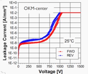
Okmetic Power GaN SOI Substrate wafers demonstrated a leakage current of 10⁻⁶ A/mm² at ~750V reverse and 850V forward bias in IMEC’s buffer breakdown voltage tests on 0.01 mm² samples.
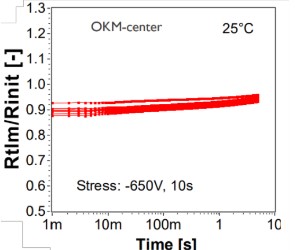
IMEC’s buffer dispersion measurements on Okmetic Power GaN SOI Substrate wafers reveal minimal trapped charge effects, with only slight curve widening, indicating excellent device performance.
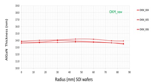
Thickness variation of the AlGaN cap layer along the wafer radius. The AlGaN cap layer demonstrated outstanding uniformity, with a consistent Al content of 21% and minimal thickness variation across the wafer.
Read more about Okmetic Power GaN Si and SOI Substrate wafers.
Read more about Okmetic RF GaN Si Substrate wafers.