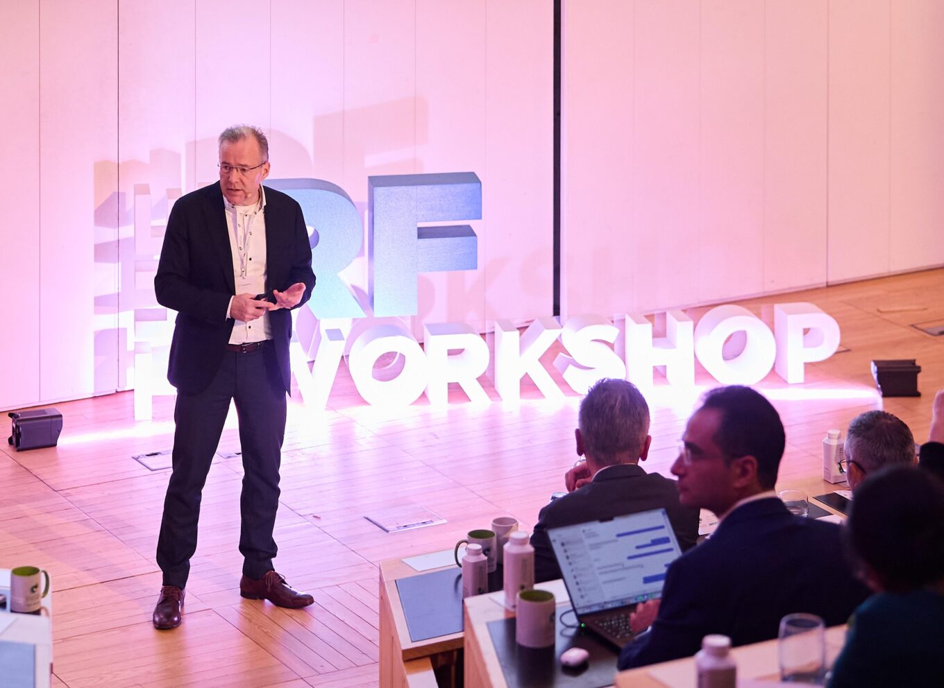
Pioneer in silicon crystals: Markku Tilli’s story
This article is the second in a series of articles about Okmetic’s 40-year history.
Markku Tilli has known Okmetic throughout its existence – and has been active in the semiconductor industry for more than 50 years. He worked at Okmetic until 2018 in several positions, most recently as Senior Vice President, Research. Aalto University awarded him honorary doctoral degree (D.Sc. h.c.) after his retirement.
Markku began his major studies in metallurgy at Helsinki University of Technology in Otaniemi in 1969. His professor was Heikki Miekk-oja, and Veikko Lindroos had been appointed assistant professor. When Miekk-oja fell ill, Veikko inherited his position, and Markku got to know Veikko more closely. In the spring of 1974, Markku completed his master’s thesis under Veikko’s guidance.
Veikko had visited an IBM conference in the USA and got ideas about silicon as a material for the future.
– Veikko got excited and suggested at the coffee table that what if we also start thinking about how we could grow silicon crystals, Markku recalls.
Markku had already started growing crystals as Veikko’s hourly assistant. He had already grown aluminum crystals, lead crystals and iron crystals. Moving on to silicon crystal growing felt natural to him.
– For quite a long time, various presentations were made with Veikko. We had a small group for which Veikko managed to arrange funding. After that, we started a full-scale project in which we built a pilot fab in the Otaniemi lab, Markku says.
The funding enabled a semiconductor metallurgical project in Otaniemi
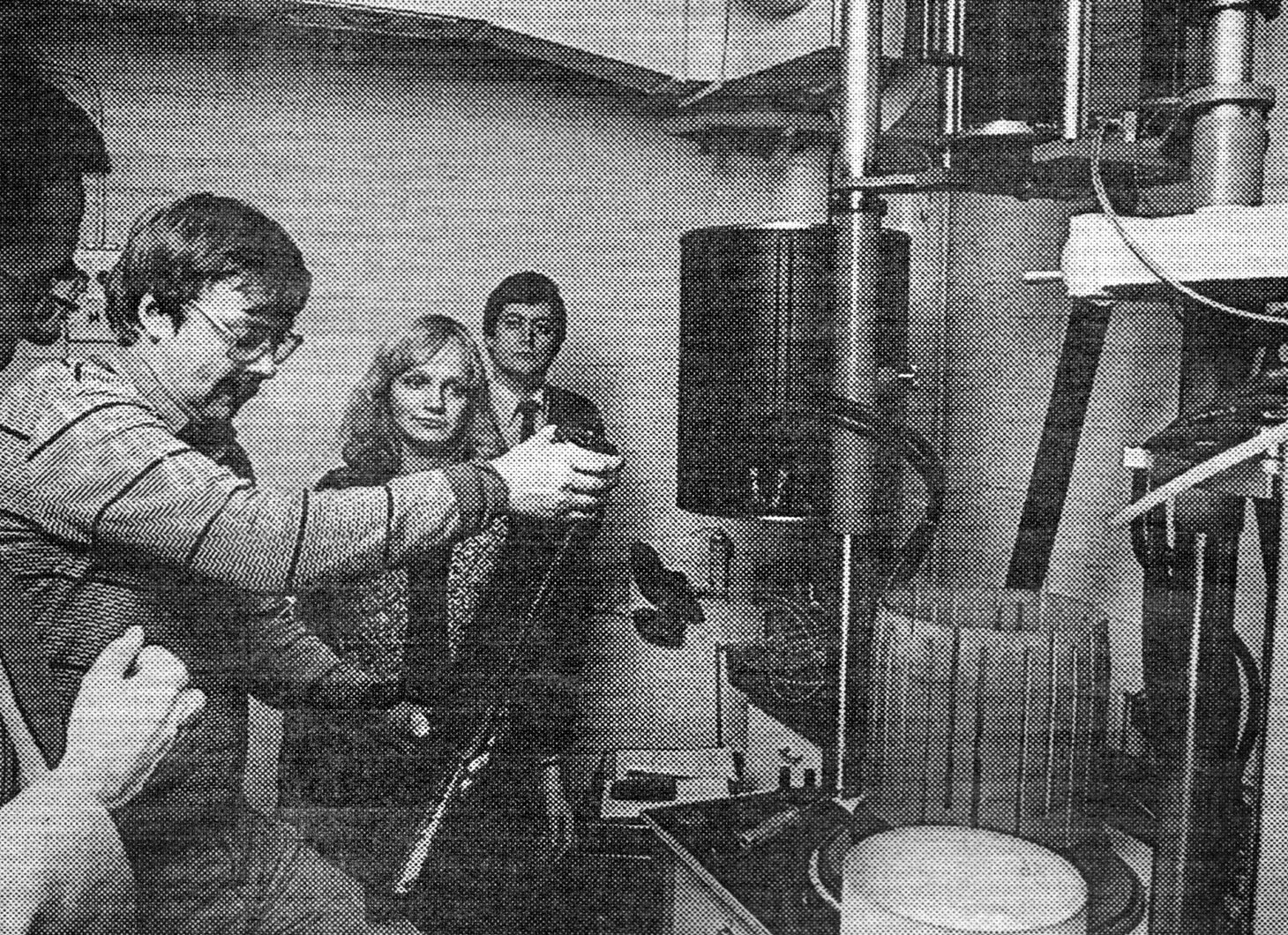
With funding from the Finnish Ministry of Trade and Industry, Outokumpu and Nokia, production equipment was purchased for the laboratory. When the semiconductor metallurgical project was launched in 1980, two master’s thesis workers were hired: Seija Hietanen for crystal growing and Karri Valvisto for crystal processing and polishing. At a later stage, a third master’s thesis worker, Simo Niklander, was hired for the same tasks as Karri. As the project expanded, Hannes Martikainen was also hired. He created the first automatic crystal growing program for the project. The crystal was grown using a PDP computer, which was a unit the size of a low office cabinet.
In April 1981, Markku and Seija travelled to the USA for a couple of weeks, where they visited a few silicon wafer fabs. The Finnish duo also got to grow silicon crystals and use a polishing machine. After the trip, the project organization ordered a lapping machine, while they decided to make the edge grinding machine themselves.
The ordered equipment arrived on 1st of May 1981, and during Midsummer week they were able to grow own silicon crystals. The first three-inch crystal was completed on Midsummer’s Eve.
– Seija was using the puller at the time, but all of us project people at the time, Karri and I, sat next to Seija. The input was then 5 kg, the hot zone was 8″ and the growing was completed in just over a working day, as we started early in the morning and everything went smoothly. There was also a person from the supplier of the puller, who guided the growing process, Markku says.
After successful crystal growing, pioneers Markku, Seija and Karri, as well as representatives of the puller supplier, went to celebrate in Seurasaari, where they raised a toast to the first silicon crystal grown in Finland.
– More than 190 crystals were grown in Otaniemi, some of which went to customers. One of our first customers was very happy with us. There was also reasonably positive feedback from another customer. At that time, we created credibility with our group in the direction of Outokumpu and Nokia.
The successful project and customer orders convinced Outokumpu’s management
In the years of 82–84, new customers were hunted for the project with the active help of Nokia and awareness was increased by supplying sample wafers to international companies. In 1983, the project received its first order when a customer satisfied with the sample wafers ordered 200 three-inch wafers. In 1984, the order books included orders for one thousand wafers from two customers and a new sample wafer order.
– We had a meeting once a month with Nokia and Outokumpu. They looked at what we would do now and what we would do in the next month. Veikko took care of his plot well, i.e. the top-level relationships, and the rest of us were able to be as free as the birds of the sky in the project, Markku says.
In 1984, Outokumpu’s Board of Directors stated that the outlook for the silicon wafer market was promising and a sales plan was drawn up: the fast-growing business would be distinguished by special products and customer service.
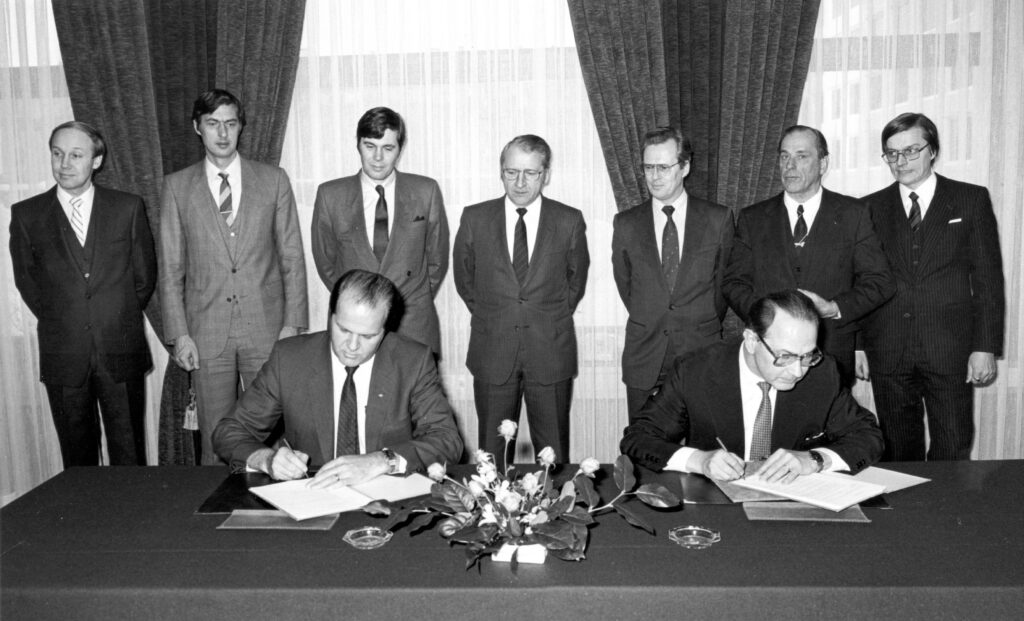
Okmetic was founded on 13.3.1985 at Hotel Intercontinental in Helsinki, when Outokumpu’s President and CEO Pertti Voutilainen and Nokia’s President and CEO Kari Kairamo signed the memorandum. The company was entered in the Trade Register on 9.5.1985.
Outokumpu’s Jukka Lehto, who was part of the semiconductor metallurgical project’s management team, came up with the name Okmetic, which stands for Outokumpu Metallurgy for Integrated Circuits.