Okmetic partaking in RF themed R&D project consortium
The project demonstrates that substrate-induced losses in RF devices are effectively mitigated by optimized silicon wafer material
Okmetic is partaking in Beetles project which is a Finnish project consortium coordinated by VTT and funded by Business Finland. In this project Okmetic is developing its low-loss high resistivity silicon substrates to meet the constantly evolving requirements of advanced RF filters and other RF devices.
The entire project consortium consists of multiple companies and research organizations such as VTT, Murata, Beneq, Emberion, CoreHW and University of Turku, and it leverages the developments in different technology platforms with multiscale modeling to realize novel RF devices. The advances in this project create a foundation for the development of novel packaging solutions for example for resonant sensors in the future.
Being one of the projects that reinforce Okmetic’s continuous RFSi® wafer development endeavors, Beetles project has successfully facilitated the development of high resistivity wafers exceeding 10 kOhm-cm, characterized by close to zero substrate-induced losses.
Product launch and new R&D insights have been key project takeaways for Okmetic
The 5G and 6G technologies set tighter requirements on RF devices in terms of losses and signal integrity, which is why new characteristics and improved performance are expected from the silicon wafers as well.
During this project, Okmetic has developed and launched Engineered Ultra High Resistivity wafer combining over 10 kOhm-cm resistivity with highly efficient trap-rich layer that mitigates the parasitic surface conduction effect. Substrate-induced losses can be very effectively suppressed by this kind of optimized silicon wafer material, which enables RF filters to reach higher linearity and lower levels of harmonic and intermodulation distortion.
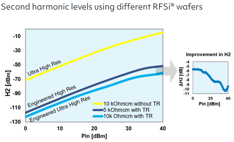
Picture 1: Substrate-induced nonlinearities in RF devices are very effectively mitigated by optimizing the silicon wafer selection
In 2021 parallel with this project, Okmetic also established a very fruitful partnership with Incize, a Belgian company specializing in semiconductor and especially RF wafer characterization. Incize’s expertise has helped Okmetic to provide its customers detailed, reliable data about the effects of different silicon wafers on RF linearity and performance.
The Beetles project has provided valuable feedback on our own high resistivity RFSi® silicon wafer research and development through collaboration with VTT and University of Turku. VTT developed and manufactured IPDs (integrated passive devices) on Okmetic low-loss silicon wafers, while University of Turku developed simulation methods for both polysilicon (trap-rich) layer growth starting from an atomistic scale and for the layers’ electromagnetic properties.
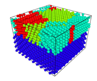
Picture 2: University of Turku investigates polysilicon growth on single crystalline silicon wafer through the use of simulation methods. This helps us understand the observed phenomena from a more complex physical perspective.
Active engagement in R&D projects helps us develop high resistivity, low-loss wafers meeting our customers’ future needs
Okmetic already has a significant share in the RF wafer market. Our comprehensive line of high resistivity RFSi® silicon wafers provides an optimal platform for the manufacture of RF filters and devices. Wafer solutions such as Engineered Ultra High Resistivity wafers, Engineered High Resistivity wafers and UF-RFSi® wafers improve RF device performance, Total Cost of Ownership and enable more ambitious designs.
The Beetles project aligns with Okmetic’s continuous RFSi® wafer development initiatives, facilitating the creation of advanced and value-added wafers to cater to the evolving needs of our customers. Our active engagement in a multitude of R&D projects enhances our comprehensive understanding on industry trends and evolving market demands.
Okmetic’s RFSi® wafer line consists of the following products:

