Okmetic Inc. President Reed gave a speech about substrates for GaN-on-Si and GaN-on-SOI at CMC Conference
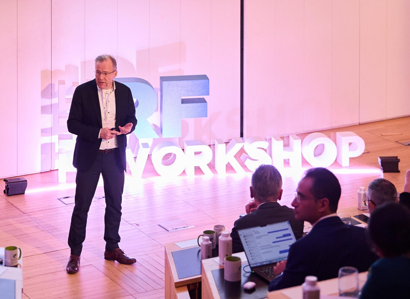
Okmetic is currently attending the Critical Materials Council (CMC) Conference held in Austin, Texas. Yesterday, Jim Reed, VP of Key Account Development and President of Okmetic Inc., gave a presentation titled “Advancing GaN Technology with Optimized Substrates: Addressing Challenges in Power and RF Applications.”
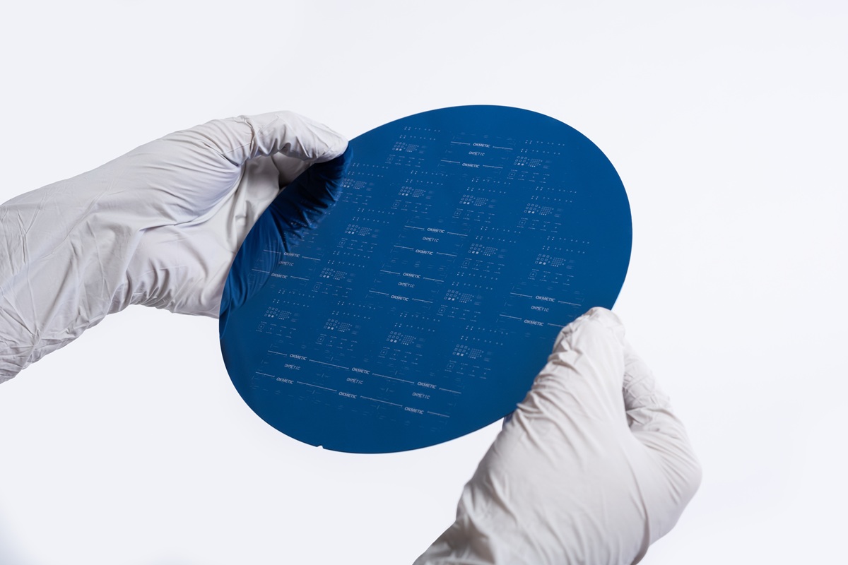
The presentation focused on how holistic wafer optimization can help resolve key GaN-on-Si challenges, including lattice and thermal mismatch, wafer bowing, and GaN layer quality – factors that are critical to device reliability and manufacturing scalability. Okmetic’s Power GaN Silicon Substrates were discussed in the context of supporting high current handling in power applications, while GaN-on-SOI substrates were presented as a promising platform for monolithic integration, offering potential for more compact and efficient device architectures.
In RF applications, the talk emphasized how RF GaN Substrates can contribute to lower insertion losses and improved signal integrity, supporting the performance needs of high-frequency systems such as 5G, 6G, and satellite communications.
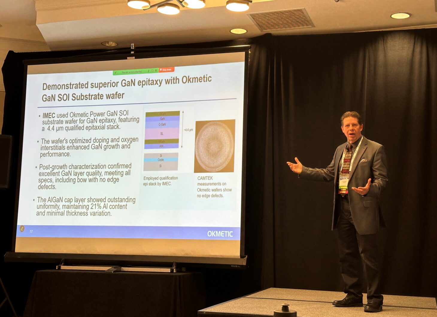
Learn more about Okmetic’s Power GaN silicon and SOI substrates and results from our recent collaboration with the Interuniversity Microelectronics Centre (IMEC) that highlight the potential of SOI wafers for GaN growth.
Learn more about RF GaN Substrate solutions.