Enhancing PMUT performance with C-SOI® and EC-SOI wafers: Results from VTT – Okmetic collaboration
Okmetic Cavity SOI (C-SOI®) and Enhanced C-SOI (EC-SOI) wafers are setting a new standard for Piezoelectric Micromachined Ultrasonic Transducers (PMUTs) and Capacitive Micromachined Ultrasonic Transducers (CMUTs). The EC-SOI wafers, which combine Okmetic Cavity SOI and E-SOI® technologies, provide exceptional uniformity in device layer thickness. This uniformity is crucial for optimizing the resonance frequency of PMUTs, as demonstrated in a recent collaboration with VTT Technical Research Centre of Finland, one of Europe’s leading research organizations. Additionally, the pre-made cavities in both EC-SOI and C-SOI® wafers make them effectively half-made devices, simplifying the manufacturing process and significantly reducing time-to-market for customers.
These recent findings are particularly noteworthy, as the benefits extend to various MEMS devices, including CMUTs, timing devices and silicon photonics, where enhanced uniformity significantly improves sensitivity and measurement accuracy.
Impact of device layer thickness uniformity on resonance frequency
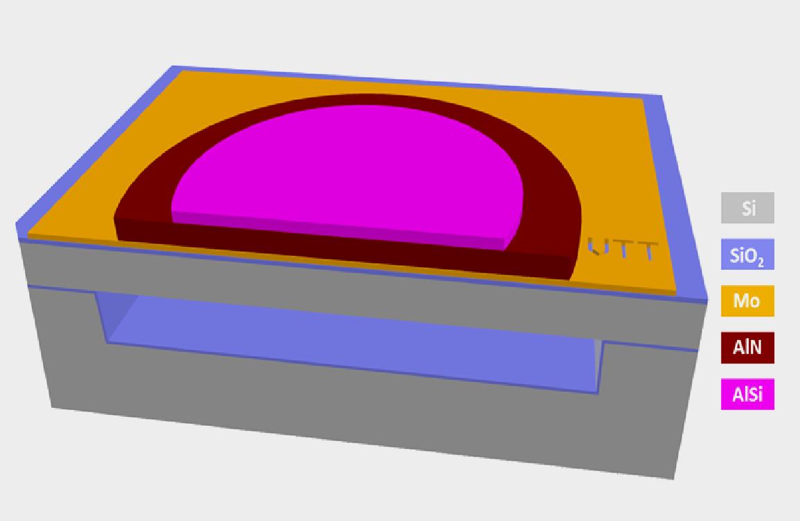
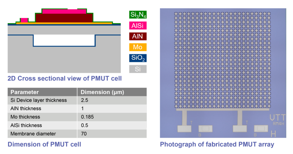
In a recent study, VTT manufactured PMUT devices on Okmetic’s C-SOI® and EC-SOI wafers to evaluate how device layer thickness uniformity affects resonance frequency. These devices, built with a 2.5 µm thick silicon layer and a 70 µm membrane diameter, operated at approximately 9.5 MHz in air (see Figure 1).

Figure 1: Cross sectional view of VTT PMUT cell built on Okmetic Cavity SOI wafer and photograph of VTT Fabricated PMUT array.
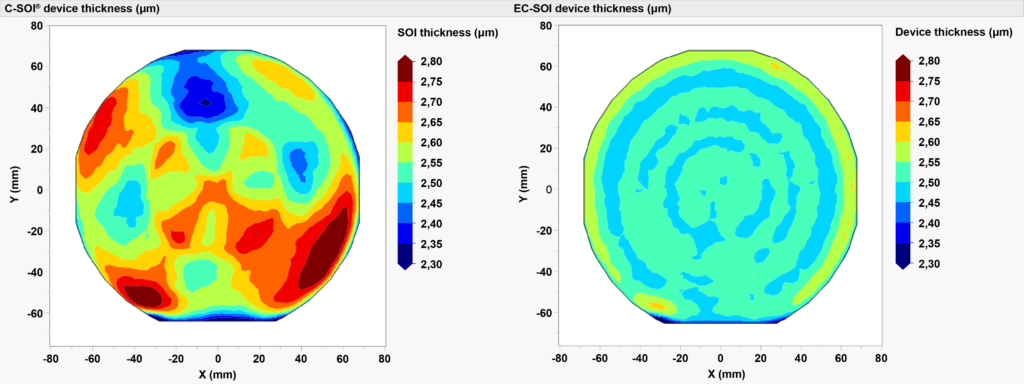
Okmetic’s C-SOI® wafers showed a thickness uniformity of 2.5 ± 0.3 µm, while EC-SOI wafers provided an enhanced uniformity of 2.5 ± 0.1 µm as seen in Figure 2. This improved uniformity in EC-SOI wafers lead to a narrower resonance frequency range, which is especially beneficial for PMUT and CMUT devices and other devices requiring high precision and specific frequency targeting.

Figure 2: Device thickness uniformity maps of C-SOI® (left) and EC-SOI wafers (right).
Comparing resonance frequency: C-SOI® vs. EC-SOI
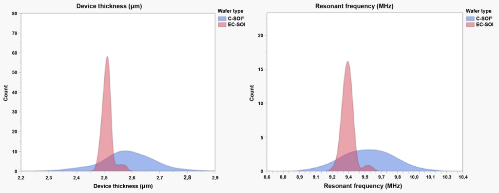
As illustrated in Figure 3, the device layer thickness distribution for EC-SOI wafers is significantly narrower than that of C-SOI® wafers. This uniformity yields a more consistent and narrower resonance frequency distribution for PMUT devices. This increased frequency selectivity enhances signal clarity, making EC-SOI wafers ideal for applications where precision and stability at specific frequencies are critical.

Figure 3: On the left, EC-SOI wafers show tighter device thickness uniformity than C-SOI® wafers, resulting in a narrower resonant frequency distribution, which is particularly beneficial for PMUTs, as illustrated on the right.
Through design and testing by VTT, Okmetic C-SOI® and EC-SOI wafers demonstrate their capacity to support the high-performance needs of PMUT devices in advanced sensing and imaging applications. The use of EC-SOI wafers enables customers to attain superior frequency precision, ensuring consistent and high-quality results across various devices.
Okmetic’s SOI wafer line comprise the following products:
- BSOI wafers – Bonded SOI (including BSOI variations 0.3 SOI, DSOI, LSOI and Thick SOI)
- C-SOI® wafers – Cavity SOI (including C-SOI® variations EC-SOI, Double C-SOI®, C-SOI® with patterned device layer, C-SOI® with poly via)
- E-SOI® wafers – Enhanced SOI with tight thickness uniformity
- Terrace Free SOI capability for BSOI, E-SOI® and Power Management SOI wafers
- High Resistivity BSOI wafers are part of our RFSi® wafer line
- Power Management SOI wafers are part of our Power wafer line


