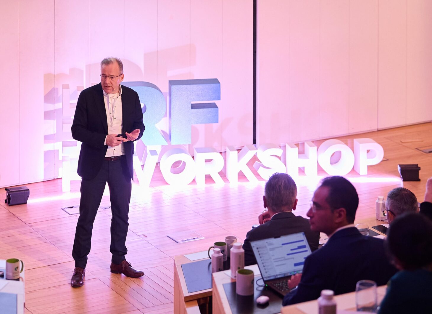
CTO Haapalinna gave a speech at Incize RF Workshop
Last week, Okmetic had the pleasure of participating in the Incize RF Workshop, an event bringing together top professionals in the RF field.
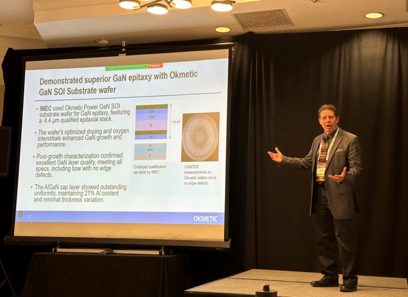
Our CTO, Dr. Atte Haapalinna, contributed to the discussion with his presentation titled “Advancing 5G and 6G with Advanced Silicon Wafers.” In his speech, he explored how optimized silicon substrates play a key role in addressing the performance demands of next-generation RF and GaN-on-Si devices.
With 5G and 6G driving the need for lower losses, enhanced linearity, wider bandwidths, higher frequencies, and new power standards, the role of substrate engineering has never been more critical. Dr. Haapalinna highlighted how Okmetic’s Engineered High Resistivity silicon wafers reduce substrate losses, improve resonator Q, and enable superior linearity, making them ideal for evolving RF architectures. He also addressed the challenges of GaN-on-Si, such as lattice and thermal mismatch, and how optimized silicon substrates can enhance GaN epitaxy and boost device reliability for both RF and power applications.
Our Engineered High Resistivity and Engineered Ultra High Resistivity wafers offer a unique combination of high bulk resistivity and a trap-rich layer that effectively suppresses both bulk and surface conductivity. This results in exceptionally low losses and excellent linearity in RF devices.
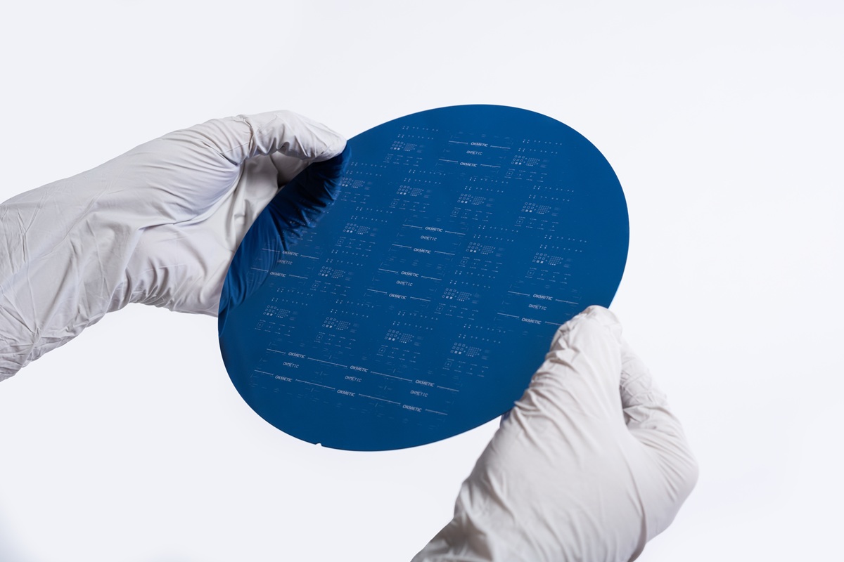
Learn more about Okmetic Power GaN Substrate wafers and RF GaN Substrate wafers.