COP level management enhancing power device reliability and yield
As technology advances and cost-effectiveness becomes increasingly critical in the power semiconductor market, the demand for high-quality wafers with enhanced performance characteristics is on the rise. Industries like automotive, renewable energy, consumer electronics, and manufacturing are fueling this demand as device manufacturers strive to reduce defects, enhance yield rates, and optimize overall device performance while maintaining cost efficiency.
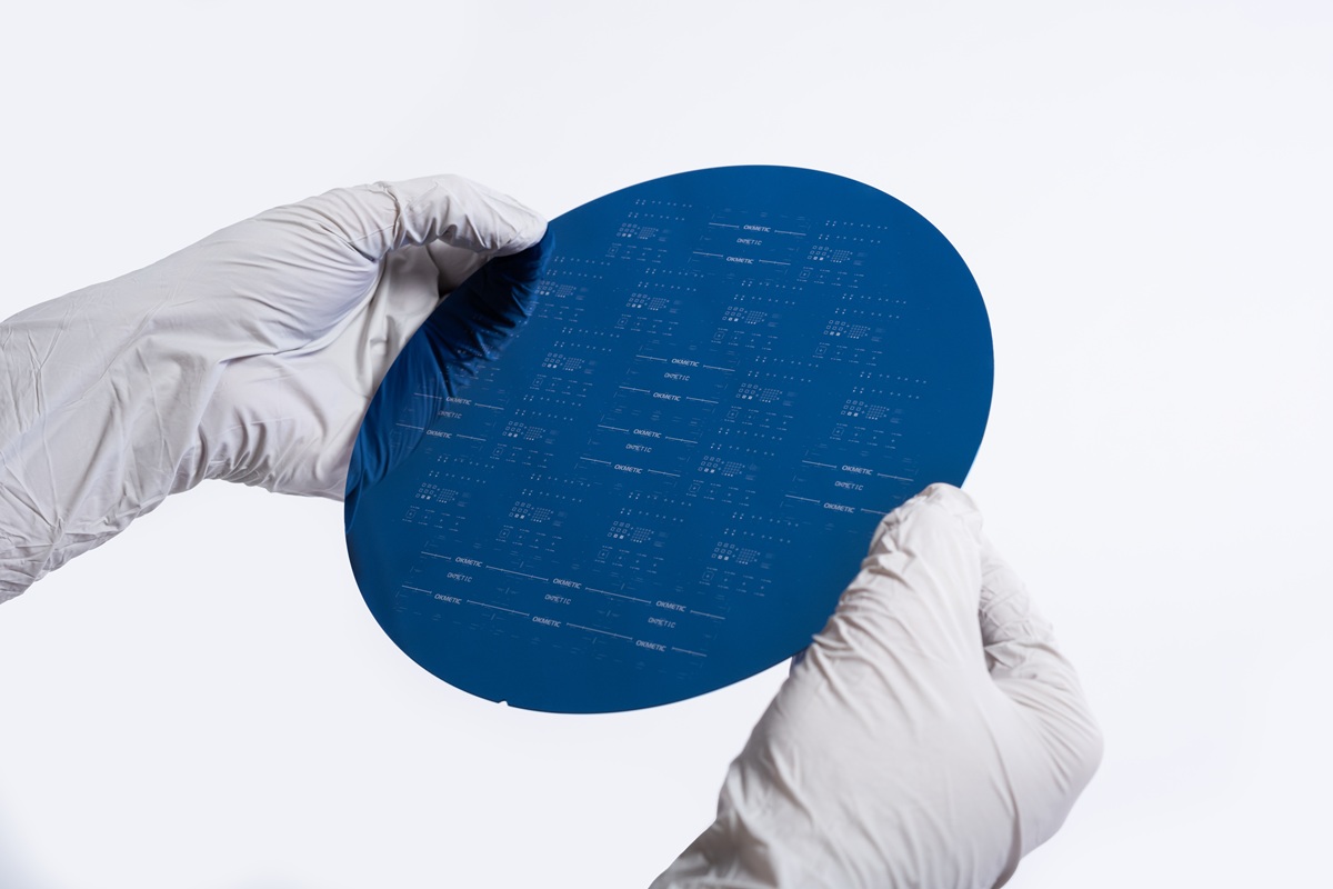
Okmetic has substantial expertise in minimizing crystal defects impacting the breakdown voltage of power devices. Our power wafers are intricately engineered to be free from dislocations and slips, but we also provide COP level management targeted for epi-free Power IC devices.
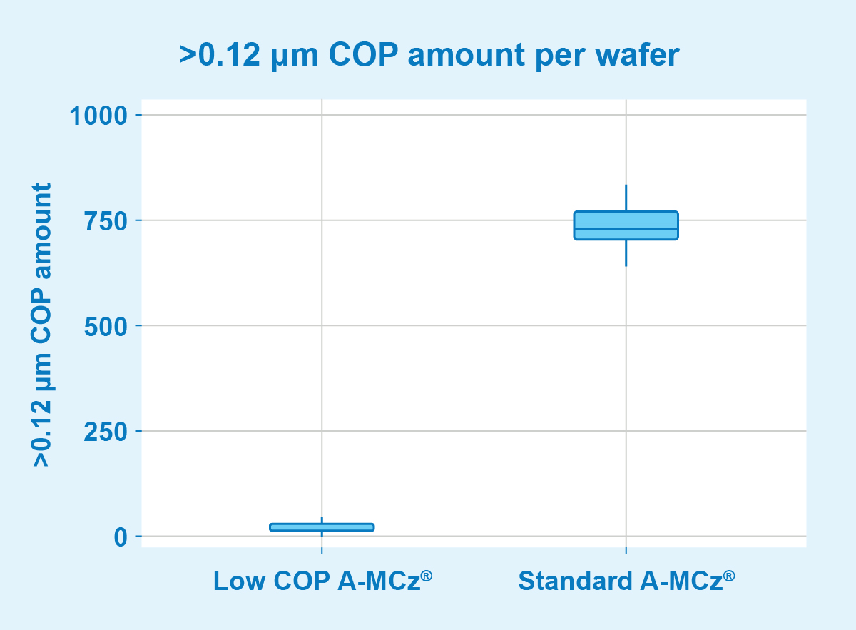
Minimized COP amount for enhanced GOI performance
Okmetic Low COP wafers are engineered to address the challenges resulting from crystal-originated particles (COPs), which can significantly impact gate oxide integrity (GOI) performance. By minimal presence of COPs near the wafer surface, our Low COP wafers enable improved yield levels and use of thinner gate oxides. Furthermore, by combining the low COP option with BMD optimization, power device manufacturers can further elevate GOI performance to meet the most demanding device requirements.
Cost-effective alternative to Float Zone wafers
Offering a cost-effective alternative to Float Zone wafers, Okmetic Low COP silicon and SOI wafers are an appealing choice for power device manufacturers seeking to streamline production processes and lower total cost of ownership. The elimination of additional, price-increasing annealing processes further enhances the cost efficiency of these wafers. The Low COP wafers are particularly well-suited for advanced NPT/FS IGBT devices and for devices that use Okmetic Power Management SOI wafers, such as gate drivers and power ASICs.
Available in 200 mm Si and SOI wafers
The Low COP wafers are manufactured using an optimized version of our signature Advanced Magnetic Czochralski (A-MCz®) crystal growth method, which reduces total cost of ownership and removes the risk of thermal stress induced slip lines normally associated with traditional COP annealing processes. Available in 200 mm Discrete Power Device and Power Management SOI wafers, Okmetic Low COP capability supports boron or phosphorus doping with resistivities above 1 Ohm-cm. In addition, Okmetic offers flexibility in meeting specification requirements and ensures compatibility with a wide range of power semiconductor devices.
Okmetic has significantly increased its Low COP wafer capacity through process optimization. Additionally, the fab expansion scheduled to be operational in early 2025 will further enhance Okmetic Low COP wafer capacity. Read more about Okmetic Low COP silicon and SOI wafers.