Advent of 5G puts new pressure on RF device and substrate development
The author is Dr. Atte Haapalinna, Chief Technology Officer of Okmetic
The world is on the cusp of mobile-network technology transformation caused by 5G and merging technologies like virtual and augmented reality. The 5G technology permits the connection of vast number of devices while enabling faster data transfer and greater capacity than with the 4G. In the uncertain future, one thing is for certain: the use of data will continue to increase exponentially along with the number of bands to cover as 5G is all about the combination of sub 6 GHz and mmWave spectrum bands.
The rising band count and higher frequencies are setting new performance standards for RF devices (Filters, Switches, Amplifiers, Antenna Tuners, IPD’s) adding pressure on new product innovations to overcome the mobile industry’s interference challenges and more stringent parameter requirements. New kind of characteristics and performance is expected also from the substrate suppliers as the entire smartphone value chain tackles to find the perfect balance between improved performance, increased functionality and cost pressures. The choice of substrate has a significant effect on RF device performance and TCO which is why the demand for tailored, process-optimized substrates has surged. Let’s have a look at what is happening on RF device frontier through the lens of substrate development.
Switches
RF Switches are predominantly made on RF SOI substrate. RF SOI will likely continue to be the winning material with product improvements launched every two or three years. RF SOI development focuses on 300mm wafers and very thin active layers.
Amplifiers
The role of amplifiers in high-end smartphone design is increasing. Amplifier designers are finding solutions for the complex problem of answering both the higher integration requirements and the physical-technical substrate challenges related to frequencies beyond those so far used in the mainstream telecommunication systems.
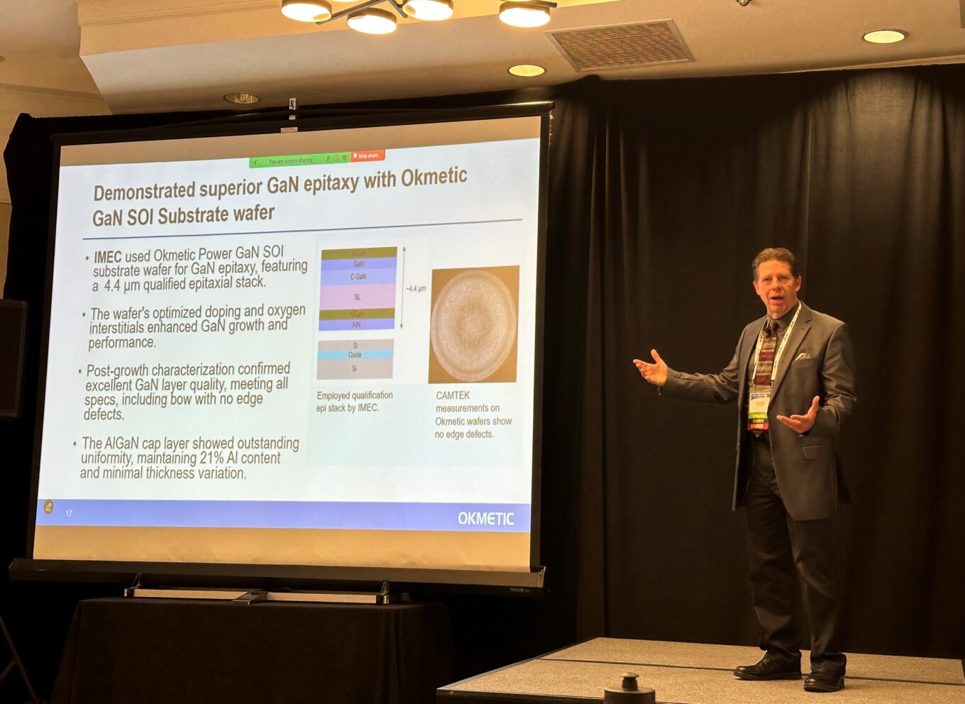
Gallium Arsenide (GaAs) is one of the traditional choice of substrates for amplifiers as it offers good efficiency and tolerates relatively high voltages. However, Gallium Nitride on Silicon (GaN on Si) is shown to be highly promising substrate for amplifiers bringing additional cost-efficiency and enabling even more efficient amplifier manufacture. GaN on Si solution is developing into increasingly competitive alternative against incumbent technology, GaN on Silicon Carbide. GaN offers performance advantages over GaAs. It works well also for higher power levels but has relatively high cost structure unless efficiency improvements can be carried out e.g. through wafer size evolution. Okmetic’s thick High Resistivity wafer has proven itself to provide an excellent substrate for high-quality GaN on Si required in latest amplifier designs.
Integrated Passive Devices for RF
The role of IPD in 5G world is increasing, and various IPD solutions are expected to form a significant part of the hardware solutions. This is true especially in the mmWave part of the spectrum in which wideband filtering and antenna adaptation will be widely utilized. Mass production of silicon-based IPDs are generally made on High Resistivity MCz wafers using standard thin film processing methods, and these benefit greatly from advanced substrates such as Okmetic offering, which is based on latest MCz and optimized passivation technologies.
Okmetic’s superior High Resistivity wafers have enabled significant improvements in demonstrated electrical performance of advanced IPD designs. Tailored, cutting-edge wafer technology reduces RF losses and provides stable effective resistivity, resulting in Q value improvements up to 250%. Besides improved linearity wafer engineering can be used to minimize and reduce characteristics such as wafer bow.
Acoustic filters: the fastest-growing RF Front End market
5G transformation is fundamentally altering the filtering requirements in RFFE design in a number of ways. New filter solutions are needed for wide but sharply defined bands, and the complicated band configurations are placing new requirements for acoustic filter performance optimization.
Bulk Acoustic Wave (BAW) filters have been the leading RF filter technology for higher frequency bands in mobile communication for several years. BAW filters currently dominate higher frequency bands up to 6 GHz, with potential extension up to 7-10 GHz range. Recently, a new type of Surface Acoustic Wave (SAW) filter, Thin Film Surface Acoustic Wave (TF SAW) filter technology, has created a very strong challenger for the BAW filter in several applications both in performance and in price. Nevertheless, continued development of BAW filter design and manufacturing processes, combined with advanced substrate materials, are a highly competitive combination. Thus BAW manufacturers believe they can meet the 5G challenges through improved filter performance and extended frequency range while at the same time maintaining or even improving the cost level. This technology competition will decide how the strong growth of filter market expected to last at least until by 2025 will be divided.
TF SAW filters are based on compound materials technology with piezoelectric material bonded on silicon handle wafers, whereas BAW filters directly utilize High Resistivity silicon wafers manufactured with either Float Zone (FZ) or Magnetic Czochralski (MCz) method. Efficiency of bond-and grindback TF SAW manufacturing process can be greatly enhanced by Ultra Flat MCz handle wafers.
Okmetic’s High Resistivity MCz wafers offer a superior option for FZ technology with enhanced performance, robustness and cost-effeciency. Okmetic also has an option for proprietary trap-rich layer on top of the High Resistivity wafer, which eliminates the need for alternative, typically implant-based passivation carried out as a part of the customer process.
Filter manufacturers have observed excellent electrical performance results with Okmetic’s High Resistivity wafers. Okmetic’s filter-optimized wafer technology can reduce substrate-related RF losses significantly and thus reliably provide high effective resistivity with improved IMD3 and second harmonics generation.
Silicon Interposers
Advancements in packaging highlight the significance of interposers and make this a growing area. Substrates typical for MEMS such as thin, patterned wafers with TSV’s have also been found to be beneficial for the manufacture of interposers. Okmetic has been supplying optimized wafers for the MEMS field for decades and interposers is a relatively new but growing market area where Okmetic can offer its expertise gained over the years.
Antenna Tuners
One of the biggest challenges with the 5G transformation will be optimization of the antenna elements, and as the number of frequency bands to cover is closing on 10, the smartphone space constraints leave little options other than tunable antenna elements. The choice of technology will be very interesting one, and among the emerging technologies both Passive Tunable Integrated Circuits (PTIC) and MEMS based tuning systems are something to follow up very closely. In the longer term, the level of complexity will almost inevitably increase, as simultaneous aperture and impedance tuning over a wide frequency range is inherently complicated.
If you are looking to improve the performance of your RF devices, having an agile R&D partner for substrate design is essential. Our technical team is at your service to discuss your needs and material parameters, and to find the best possible solution for you.


