20 years of C-SOI®: Enabling streamlined production of high-performance MEMS devices
In 2025, we proudly celebrate two decades of Cavity SOI (C-SOI®) wafer production, a milestone that marks a significant evolution in MEMS technology. Since its launch in 2005, Okmetic’s C-SOI® wafers have been at the forefront of MEMS and sensor advancements, meeting the industry’s growing demands for precision, reliability, integration, and cost-efficiency.
As a foundational technology in MEMS manufacturing, our C-SOI® wafers enable streamlined production, reduced complexity, and enhanced efficiency. The wafers’ unique structure allows for smaller die sizes and improved yield, directly lowering costs while enhancing device performance.
Okmetic C-SOI® technology has driven a sharp increase in the use of MEMS and sensor devices in recent years, following steady growth over the past decades. Our C-SOI® wafers are widely used in a variety of MEMS applications, including pressure sensors, microphones, inertial sensors and measurement units (IMUs), offering high precision and accuracy. They also enable compact, high-performance optical devices, actuators, timing/resonating devices and are well-suited for RF switches and RF timing devices.
C-SOI® enabling high precision, cost-efficient, and compact MEMS design
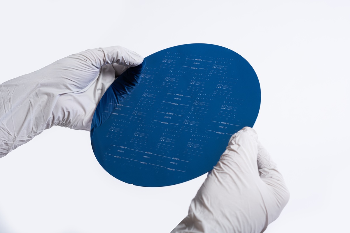
C-SOI® is a bonded Cavity Silicon-On-Insulator wafer with built-in sealed cavities. These cavities are patterned and etched on either the bottom handle wafer or the buried oxide (BOX) layer before bonding and thinning the top silicon wafer, which serves as the device layer.
More than just a wafer, C-SOI® functions like a partially built sensor, making it an optimal platform for MEMS. It offers multiple benefits, including:
- Integrated cavities and design flexibility: Customizable cavities enable direct integration of movable parts like membranes and sensors, allowing complex, high-functionality designs.
- Streamlined manufacturing and cost efficiency: C-SOI® reduces process steps, enhances reliability, and lowers production costs, accelerating time to market.
- Superior performance and precision: Designed with precisely engineered cavities and a layered structure, including a buried oxide layer for excellent electrical isolation, C-SOI® wafers enhance device performance and precision, making them ideal for high-precision MEMS applications.
- Enhanced reliability and yield: All the C-SOI® handle wafers undergo AVI inspection for enhanced quality assurance and the bond quality is confirmed with scanning acoustic microscope. Okmetic’s expertise in patterning and bonding along with above inspections ensures high yield and enhanced reliability for our customers’ devices.
- Compact and highly integrated design: C-SOI® supports multiple functionalities on a single wafer, reducing chip size by up to two-thirds.
Customized C-SOI® solutions advancing MEMS with innovation
Okmetic expertise in Cavity SOI technology provides highly customizable wafers tailored to meet the specific requirements of each customer’s device and process. Our solutions include options such as double device layers, patterned device layers, poly filled TSVs, and highly uniform device layers, ensuring precise and efficient designs for complex MEMS structures.
One of the most popular solutions is EC-SOI, which combines the advanced properties of highly uniform device layer thickness in E-SOI® wafers with the embedded cavity structures of C-SOI®. This innovative substrate opens up new possibilities for cutting-edge MEMS devices. Read more about usage benefits in silicon photonic integrated circuits (PICs) and ultrasonic transducers, such as PMUTs and CMUTs.
To support the tailored solutions, Okmetic has a fully in-house Cavity SOI® process that covers every step from crystal growth and wafering to photolithography, deep reactive-ion etching (DRIE), and bonding. This control over the entire process guarantees the highest quality and precision. As part of our customization options, we can make alignment marks on the front or backside of the C-SOI® wafer to help customers align their processes with the pre-made cavities by Okmetic.
With ongoing R&D and close customer collaboration, Okmetic is committed to advancing C-SOI® technology, meeting the growing demand for high-performance, customized wafer solutions in the evolving MEMS and sensor industries. The journey of C-SOI® is just getting started!


