News & insights
Select content category
Okmetic Customer Technical Support Manager Akiko Gädda succesfully defended the dissertation
Okmetic’s Päivi Sievilä is giving a speech at Microfab Summit on 2-4 November
Technology Manager Päivi Sievilä can utilize her diverse experience in her new position
VTT organizes a virtual event Boosting growth with Finnish microelectronics on 20 May 2021 – Okmetic’s CTO participates in the panel discussion
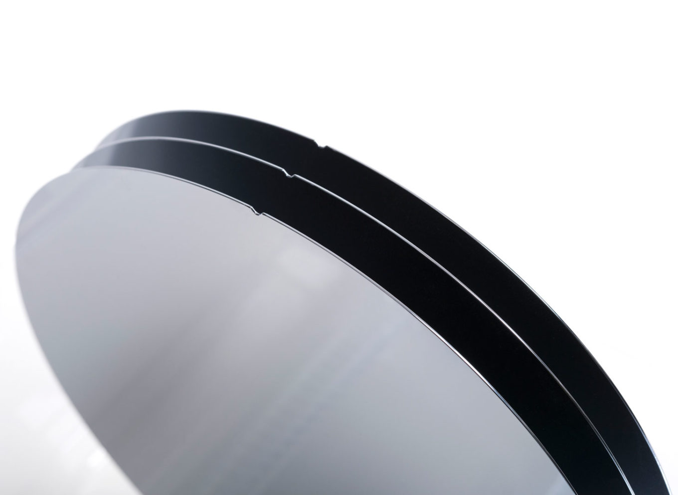
20 years of Okmetic SOI wafers – Bonded SOI wafers enable more ambitious device designs cost-effectively
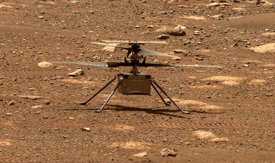
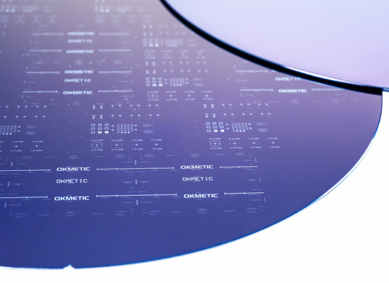
Mars exploration is enabled with sensor technology by Murata Finland using Okmetic’s advanced silicon wafer as a platform
Okmetic is now one of Finland’s 500 largest companies

Okmetic participates in an EU project in which AI is utilized to improve the reliability of electronics

Okmetic’s corporate social responsibility report 2020 has been published
Product Release: Okmetic Expands Its RFSi™ Portfolio with Tailored Silicon Substrate for Thin Film Surface Acoustic Wave Hybrid Structures
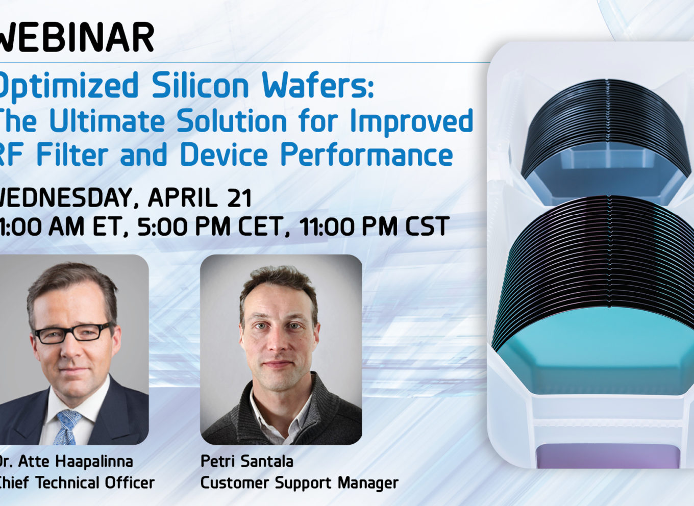
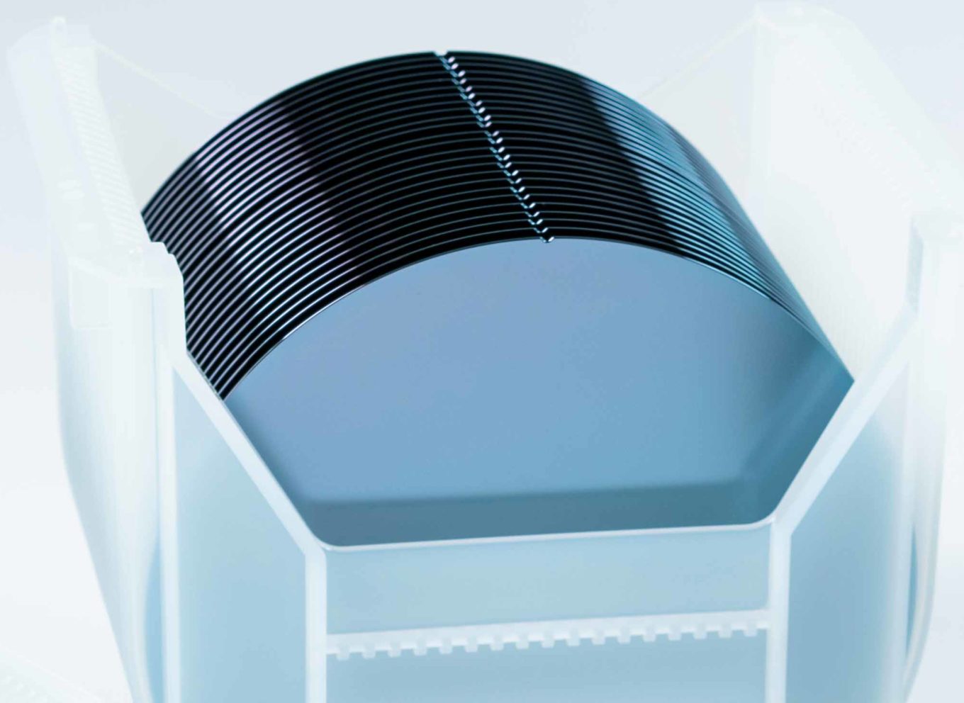
Upcoming Webinar – Optimized Silicon Wafers: The Ultimate Solution for Improved RF filter and Device Performance

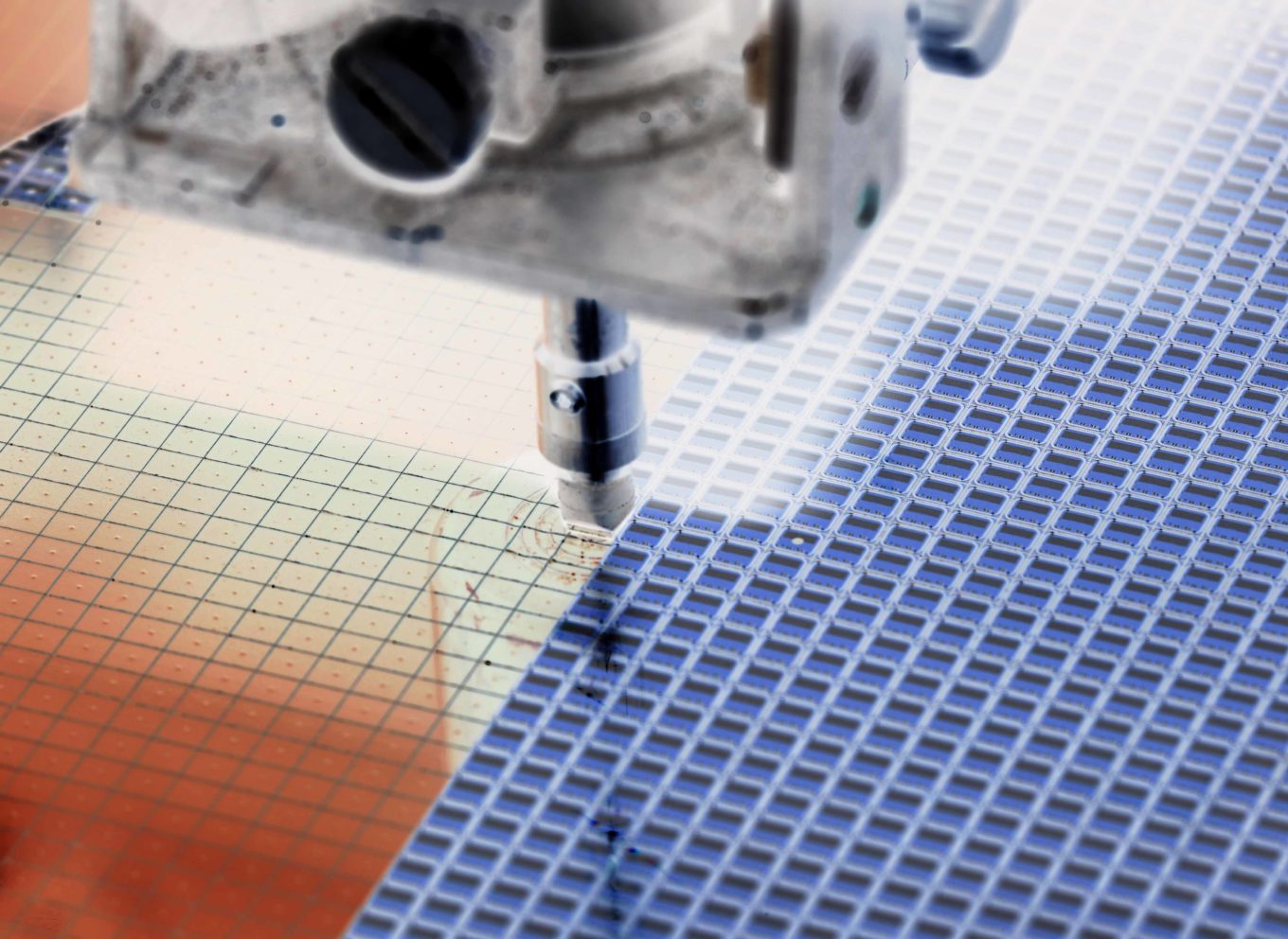
Advent of 5G puts new pressure on RF device and substrate development
Technology and Trends: SEMI blog by Heikki Holmberg
Okmetic is attending Sense’19 held on 9-10 October